CYDC256B16, CYDC128B16, CYDC064B16, CYDC128B08, CYDC064B08
When reading a semaphore, all sixteen/eight data lines output the semaphore value. The read value is latched in an output register to prevent the semaphore from changing state during a write from the other port. If both ports attempt to access the semaphore within tSPS of each other, the semaphore will definitely be obtained by one side or the other, but there is no guarantee which side will control the semaphore. On
Architecture
The CYDC256B16, CYDC128B16, CYDC064B16, CYDC128B08, CYDC064B08 consist of an array of 4k, 8k, or 16k words of 16
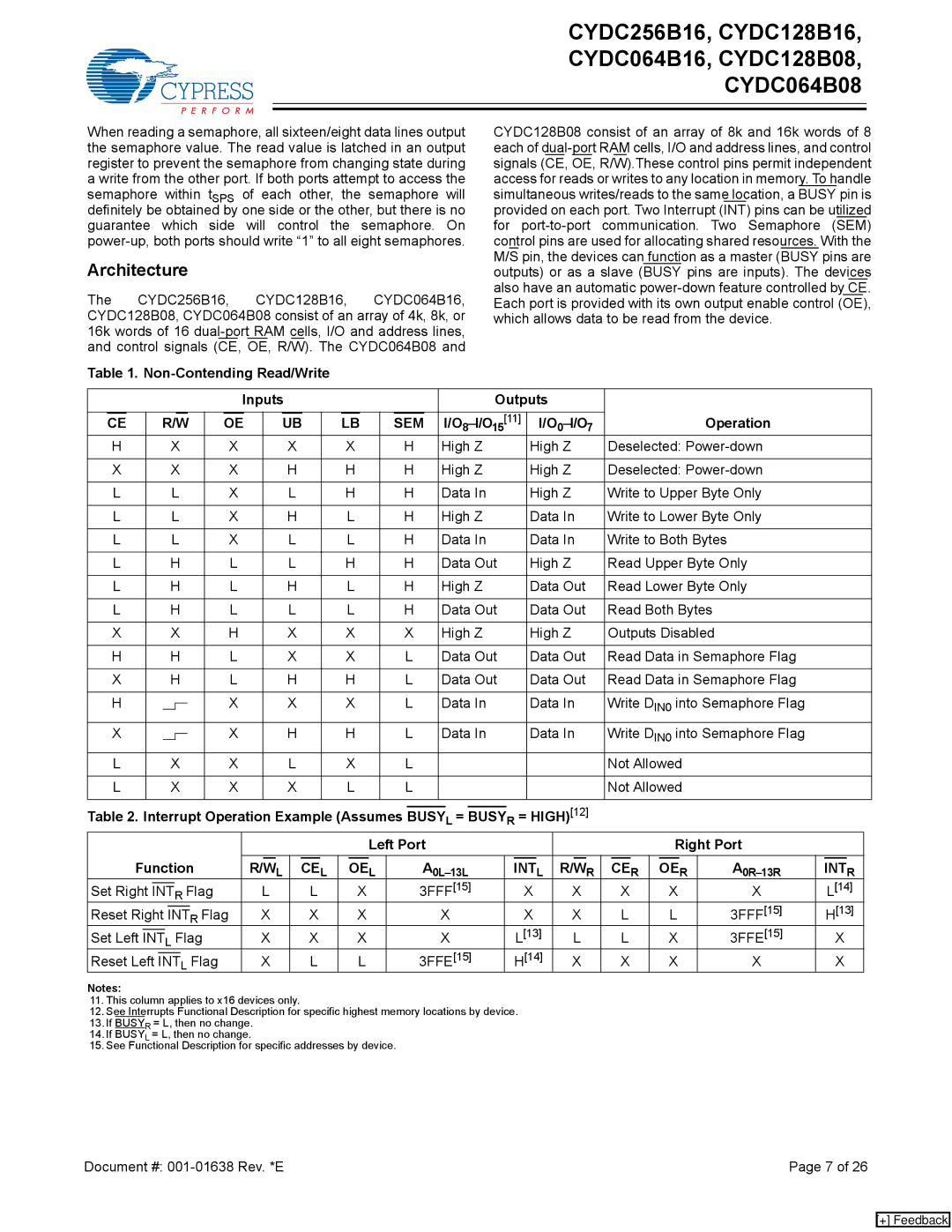
Table 1. Non-Contending Read/Write
CYDC128B08 consist of an array of 8k and 16k words of 8 each of
|
|
|
|
|
|
|
|
|
|
|
|
|
|
|
|
| Inputs |
|
|
|
|
|
|
|
|
|
|
|
|
|
|
|
|
|
| Outputs |
|
|
|
|
|
|
|
|
|
|
|
|
|
|
|
| |||||||||
|
|
|
|
|
|
|
|
|
|
|
|
|
|
|
|
|
|
|
|
|
|
|
|
|
|
|
|
|
|
|
|
|
|
|
|
|
|
|
|
|
|
|
|
|
|
|
|
|
|
|
|
|
|
|
|
| |||||
| CE |
|
|
|
|
| R/W |
|
|
| OE |
|
|
| UB |
|
| LB |
|
| SEM | I/O | [11] | I/O |
|
|
|
|
|
| Operation |
|
|
| |||||||||||||||||||||||||||
|
|
|
|
|
|
|
|
|
|
|
|
|
|
|
|
|
|
|
|
|
|
|
|
|
|
|
|
|
|
|
|
|
|
|
| 8 | 15 |
| 0 | 7 |
|
|
|
|
|
|
|
|
|
|
|
|
| ||||||||
| H |
|
|
|
|
|
|
| X |
| X |
|
|
|
| X |
|
| X |
|
| H | High Z |
|
|
|
| High Z |
|
|
|
| Deselected: |
|
|
| |||||||||||||||||||||||||
|
|
|
|
|
|
|
|
|
|
|
|
|
|
|
|
|
|
|
|
|
|
|
|
|
|
|
|
|
|
|
|
|
|
|
|
|
|
|
|
|
|
|
| ||||||||||||||||||
| X |
|
|
|
|
|
|
| X |
| X |
|
|
|
| H |
|
| H |
|
| H | High Z |
|
|
|
| High Z |
|
|
|
| Deselected: |
|
|
| |||||||||||||||||||||||||
|
|
|
|
|
|
|
|
|
|
|
|
|
|
|
|
|
|
|
|
|
|
|
|
|
|
|
|
|
|
|
|
|
|
|
|
|
|
|
|
|
|
|
| ||||||||||||||||||
| L |
|
|
|
|
|
|
| L |
| X |
|
|
|
| L |
|
| H |
|
| H | Data In |
|
|
|
| High Z |
|
|
|
| Write to Upper Byte Only |
|
|
| |||||||||||||||||||||||||
|
|
|
|
|
|
|
|
|
|
|
|
|
|
|
|
|
|
|
|
|
|
|
|
|
|
|
|
|
|
|
|
|
|
|
|
|
|
|
|
| |||||||||||||||||||||
| L |
|
|
|
|
|
|
| L |
| X |
|
|
|
| H |
|
| L |
|
| H | High Z |
|
|
|
| Data In | Write to Lower Byte Only |
|
|
| |||||||||||||||||||||||||||||
|
|
|
|
|
|
|
|
|
|
|
|
|
|
|
|
|
|
|
|
|
|
|
|
|
|
|
|
|
|
|
|
|
|
|
|
|
|
|
|
|
| ||||||||||||||||||||
| L |
|
|
|
|
|
|
| L |
| X |
|
|
|
| L |
|
| L |
|
| H | Data In |
|
|
|
| Data In | Write to Both Bytes |
|
|
|
|
| |||||||||||||||||||||||||||
|
|
|
|
|
|
|
|
|
|
|
|
|
|
|
|
|
|
|
|
|
|
|
|
|
|
|
|
|
|
|
|
|
|
|
|
|
|
|
|
|
|
| |||||||||||||||||||
| L |
|
|
|
|
|
|
| H |
| L |
|
|
|
| L |
|
| H |
|
| H | Data Out |
|
|
| High Z |
|
|
|
| Read Upper Byte Only |
|
|
| ||||||||||||||||||||||||||
|
|
|
|
|
|
|
|
|
|
|
|
|
|
|
|
|
|
|
|
|
|
|
|
|
|
|
|
|
|
|
|
|
|
|
|
|
|
|
|
| |||||||||||||||||||||
| L |
|
|
|
|
|
|
| H |
| L |
|
|
|
| H |
|
| L |
|
| H | High Z |
|
|
|
| Data Out | Read Lower Byte Only |
|
|
| |||||||||||||||||||||||||||||
|
|
|
|
|
|
|
|
|
|
|
|
|
|
|
|
|
|
|
|
|
|
|
|
|
|
|
|
|
|
|
|
|
|
|
|
|
|
|
|
| |||||||||||||||||||||
| L |
|
|
|
|
|
|
| H |
| L |
|
|
|
| L |
|
| L |
|
| H | Data Out |
|
|
| Data Out | Read Both Bytes |
|
|
|
|
| ||||||||||||||||||||||||||||
|
|
|
|
|
|
|
|
|
|
|
|
|
|
|
|
|
|
|
|
|
|
|
|
|
|
|
|
|
|
|
|
|
|
|
|
|
|
|
|
|
|
|
|
| |||||||||||||||||
| X |
|
|
|
|
|
|
| X |
| H |
|
|
|
| X |
|
| X |
|
| X | High Z |
|
|
|
| High Z |
|
|
|
| Outputs Disabled |
|
|
|
|
| |||||||||||||||||||||||
|
|
|
|
|
|
|
|
|
|
|
|
|
|
|
|
|
|
|
|
|
|
|
|
|
|
|
|
|
|
|
|
|
|
|
|
|
|
|
| ||||||||||||||||||||||
| H |
|
|
|
|
|
|
| H |
| L |
|
|
|
| X |
|
| X |
|
| L | Data Out |
|
|
| Data Out | Read Data in Semaphore Flag |
|
|
| ||||||||||||||||||||||||||||||
|
|
|
|
|
|
|
|
|
|
|
|
|
|
|
|
|
|
|
|
|
|
|
|
|
|
|
|
|
|
|
|
|
|
|
|
|
|
|
| ||||||||||||||||||||||
| X |
|
|
|
|
|
|
| H |
| L |
|
|
|
| H |
|
| H |
|
| L | Data Out |
|
|
| Data Out | Read Data in Semaphore Flag |
|
|
| ||||||||||||||||||||||||||||||
|
|
|
|
|
|
|
|
|
|
|
|
|
|
|
|
|
|
|
|
|
|
|
|
|
|
|
|
|
|
|
|
|
|
|
|
|
|
|
|
|
|
| |||||||||||||||||||
| H |
|
|
|
|
|
|
|
|
|
|
|
|
| X |
|
|
|
| X |
|
| X |
|
| L | Data In |
|
|
|
| Data In | Write DIN0 into Semaphore Flag |
|
|
| |||||||||||||||||||||||||
|
|
|
|
|
|
|
|
|
|
|
|
|
|
|
|
|
|
|
|
|
|
|
|
|
|
|
|
| |||||||||||||||||||||||||||||||||
|
|
|
|
|
|
|
|
|
|
|
|
|
|
|
|
|
|
|
|
|
|
|
|
|
|
|
|
| |||||||||||||||||||||||||||||||||
| X |
|
|
|
|
|
|
|
|
|
|
|
|
| X |
|
|
|
| H |
|
| H |
|
| L | Data In |
|
|
|
| Data In | Write DIN0 into Semaphore Flag |
|
|
| |||||||||||||||||||||||||
|
|
|
|
|
|
|
|
|
|
|
|
|
|
|
|
|
|
|
|
|
|
|
|
|
|
|
|
| |||||||||||||||||||||||||||||||||
|
|
|
|
|
|
|
|
|
|
|
|
|
|
|
|
|
|
|
|
|
|
|
|
|
|
|
|
| |||||||||||||||||||||||||||||||||
| L |
|
|
|
|
|
|
| X |
| X |
|
|
|
| L |
|
| X |
|
| L |
|
|
|
|
|
|
|
|
|
|
|
|
|
| Not Allowed |
|
|
|
|
| |||||||||||||||||||
|
|
|
|
|
|
|
|
|
|
|
|
|
|
|
|
|
|
|
|
|
|
|
|
|
|
|
|
|
|
|
|
|
|
|
|
|
|
|
|
|
|
|
|
|
|
|
| ||||||||||||||
| L |
|
|
|
|
|
|
| X |
| X |
|
|
|
| X |
|
| L |
|
| L |
|
|
|
|
|
|
|
|
|
|
|
|
|
| Not Allowed |
|
|
|
|
| |||||||||||||||||||
|
|
|
|
|
|
|
|
|
|
|
|
|
|
|
|
|
|
|
|
|
|
|
|
|
|
|
|
|
|
|
|
| |||||||||||||||||||||||||||||
Table 2. Interrupt Operation Example (Assumes |
|
|
| L = |
|
|
| R = HIGH)[12] |
|
|
|
|
|
|
|
|
|
|
|
| |||||||||||||||||||||||||||||||||||||||||
BUSY | BUSY |
|
|
|
|
|
|
|
|
|
|
|
| ||||||||||||||||||||||||||||||||||||||||||||||||
|
|
|
|
|
|
|
|
|
|
|
|
|
|
|
|
|
|
|
|
|
|
|
|
|
|
|
|
| Left Port |
|
|
|
|
|
|
|
|
|
|
|
|
|
|
|
|
|
| Right Port |
|
|
| ||||||||||
|
|
| Function |
| R/W | L |
|
| CEL |
|
| OEL |
|
|
|
|
| INTL | R/WR |
|
| CER |
| OER |
|
| INTR |
| |||||||||||||||||||||||||||||||||
Set Right |
|
|
|
|
| R Flag |
| L |
|
|
| L |
|
| X |
|
| 3FFF[15] |
|
|
| X |
| X |
|
| X |
| X |
| X |
| L[14] |
| |||||||||||||||||||||||||||
INT |
|
|
|
|
|
|
|
|
|
| |||||||||||||||||||||||||||||||||||||||||||||||||||
Reset Right |
|
|
|
| R Flag | X |
|
|
| X |
|
| X |
|
|
|
| X |
|
|
| X |
| X |
|
| L |
| L |
| 3FFF[15] |
| H[13] |
| |||||||||||||||||||||||||||
INT |
|
|
|
|
|
|
|
|
|
|
| ||||||||||||||||||||||||||||||||||||||||||||||||||
Set Left |
|
|
|
|
| L Flag |
| X |
|
|
| X |
|
| X |
|
|
|
| X |
|
|
| L[13] |
| L |
|
| L |
| X |
| 3FFE[15] |
| X |
| |||||||||||||||||||||||||
INT |
|
|
|
|
|
|
|
|
|
|
|
| |||||||||||||||||||||||||||||||||||||||||||||||||
Reset Left |
|
|
|
|
| L Flag |
| X |
|
|
| L |
|
| L |
|
| 3FFE[15] |
|
|
| H[14] |
| X |
|
| X |
| X |
| X |
| X |
| |||||||||||||||||||||||||||
INT |
|
|
|
|
|
|
|
|
|
| |||||||||||||||||||||||||||||||||||||||||||||||||||
Notes:
11.This column applies to x16 devices only.
12.See Interrupts Functional Description for specific highest memory locations by device.
13.If BUSYR = L, then no change.
14.If BUSYL = L, then no change.
15.See Functional Description for specific addresses by device.
Document #: | Page 7 of 26 |
[+] Feedback