Installing and Configuring the EVGA nForce 680i SLI Motherboard
Memory Timing
This section of the Adjust Motherboard Settings allows you to adjust various memory timings and cycles.
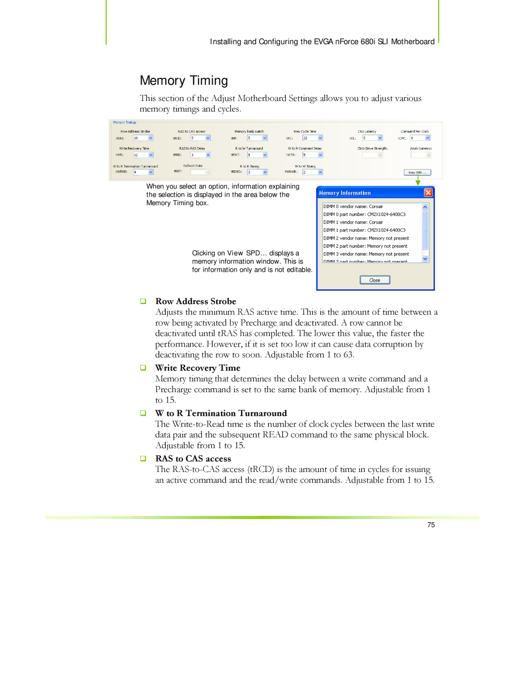
When you select an option, information explaining the selection is displayed in the area below the Memory Timing box.
Clicking on View SPD… displays a memory information window. This is for information only and is not editable.
Row Address Strobe
Adjusts the minimum RAS active time. This is the amount of time between a row being activated by Precharge and deactivated. A row cannot be deactivated until tRAS has completed. The lower this value, the faster the performance. However, if it is set too low it can cause data corruption by deactivating the row to soon. Adjustable from 1 to 63.
Write Recovery Time
Memory timing that determines the delay between a write command and a Precharge command is set to the same bank of memory. Adjustable from 1 to 15.
W to R Termination Turnaround
The
RAS to CAS access
The
75