MS/s, 12-bit, 16-ch High- Speed Multifunction Card
PCI-1712/1712L Quick Start Unpacking
Device Installation
Page
Contents
Calibration
Appendix D. Register Structure and Format
100
Figures
Auto A/D Calibration Dialog Box
I/O Connector Signal Description Part
Corresponding Full Scale values for various Input
Table D-1PCI-1712/1712L register format Part Table D-2
Table D-3
101
100
102
Page
Features
Introduction
PCI-Bus Mastering Data Transfer
Plug-and-Play Function
On-board Fifo Memory
Automatic Channel/Gain/SD*/BU* Scanning
On-board Programmable Multifunction Counter/Timer
Installation Guide
Continuous Analog Output
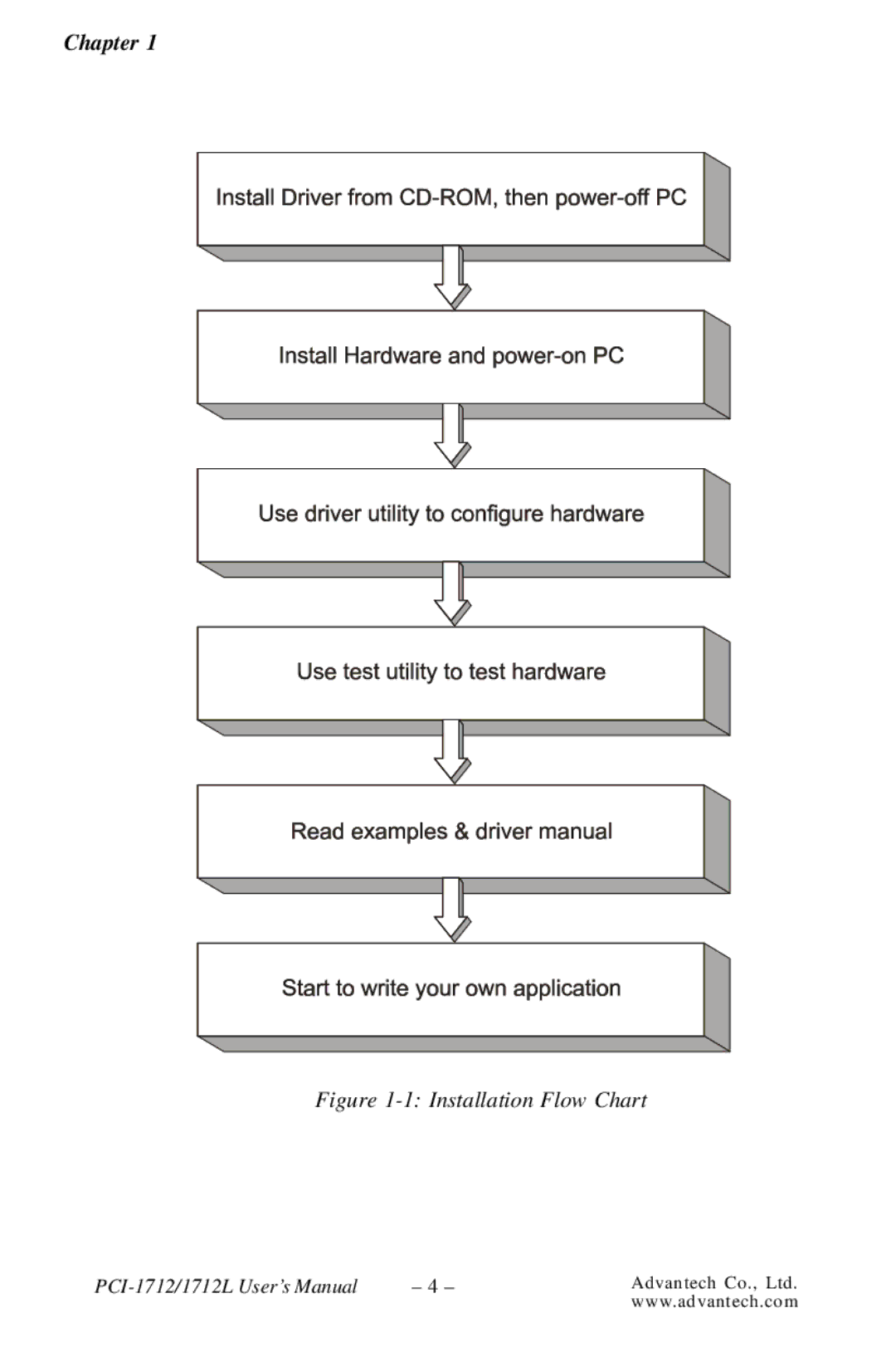
Installation Flow Chart
Wiring Cable
Accessories
Wiring Boards
Chapter
Installation
Unpacking
Driver Installation
Setup Screen of Advantech Automation Software
Hardware Installation
Different options for Driver Setup
Chapter
Device name listed on the Device Manager
Device Setup & Configuration
Setting Up the Device
Configuring the Device
Devices Found dialog box
For unipolar
For bipolar
Device Testing
Testing Analog Input Function
Testing Analog Output Function PCI-1712 only
Testing Digital Input Function
Testing Digital Output Function
Testing Counter Function
14 Digital output tab on the Device Test dialog box
Signal Connections
I/O Connector
Overview
Pin Assignment
I/O connector pin assignments for the PCI-1712/1712L
Connector Signal Description
I/O Connector Signal Description Part
Signal Name Reference Direction Description
Counter 0 Gate Input. This pin is for
Single-ended Channel Connections
Analog Input Connections
Differential Channel Connections
Chapter
Differential input channel connection floating signal Source
Analog Output Connections
Analog output connections
Field Wiring Considerations
Software Overview
Programming Choices
DLL Driver
Register-level Programming
DLL Driver Programming Roadmap
Programming Tools
Troubleshooting DLL Driver Error
Programming with DLL Driver Function Library
Chapter
Analog Input Features
Principles of Operation
Analog Input Ranges and Gains
Gains and Analog Input Range
Analog Input Acquisition Modes
Post-Trigger Acquisition Mode
About-Trigger Acquisition Mode
Pre-Trigger Acquisition Mode
Sample Clock Sources
PCI-1712/1712L Sample Clock Source
Trigger Sources
Analog Input Data Format
Analog Input Data Format
Analog Output Ranges
Analog Output Features
Analog Output Operation Modes
Output Clock Sources
Trigger Sources
Analog Output Data Format
Digital I/O Features
Analog Output Data Format
Counter/Timer Features
Clock sources
Gate Types and Sources
Counter/timer operation modes
Chapter
Chapter
Frequency measurement
Chapter
Chapter
Pulse width measurement
Internal, and gate use for pulse
Show the duty ratio of positive
Calibration
VR Assignment
A/D Calibration
D/A Calibration
Calibration Utility
Selecting the device you want to calibrate
Channel Auto-Calibration
Auto A/D Calibration Dialog Box
A/D Calibration Procedure
A/D Calibration is finished
Range Selection in D/A Calibration
11 Calibrating D/A Channel
Channel Manual-Calibration
13 Selecting Input Rage in Manual A/D Calibration panel
14 Adjusting registers
15 & -16 Selecting D/A Range Choosing Output Voltage
17 Adjusting registers
Chapter
Specification
Analog Input
Analog Output PCI-1712 only
Digital Input /Output
Counter/Timer
General
Appendix a
Block Diagram
Block Diagram
Appendix B
Screw-terminal Board
Board Layout
Pin Assignment
Figure C-2 CN2 pin assignments for the PCLD-8712
Single-ended Connections
Differential Connections
Register Structure and Format
I/O Port Address Map
Appendix D
Table D-1 PCI-1712/1712L register format Part
Base PCI-1712/1712L Register Format Address
Channel data for continuous output operation mode 30 W
A/D Single Value Acquisition Write BASE+0
Channel and A/D data Read Base +
Data of A/D Conversion
CH2 to CH0 Channel Number
A/D Channel Range Setting Write BASE+2
Table D-3 Register for A/D channel range setting
Single-ended or Differential
Bipolar or Unipolar
MUX Control Write BASE+4
Table D-4 Gain Codes for the PCI-1712/1712L
Table D-5 Register for multiplexer control
Start Scan Channel Number
Appendix D
A/D Control/Status Register Write/Read BASE+6
Analog input acquisition mode register
Table D-6 Register for A/D control/status
Sample clock source select register
Trigger source control register
Trigger edge control register
Analog I/O calibration bit
Clear interrupt and Fifo Write BASE+8
Aitrgf Analog input trigger flag
Table D-8 Register for clear interrupt and Fifo
Clear A/D Fifo
Interrupt and Fifo status Read BASE+8
Interrupt flag
Fifo empty flag
Fifo half-full flag
10 D/A control/status register Write/Read BASE+A
Table D-11 Analog output operation mode
Channel 1 unipolar or bipolar output
Clock source select register
Aotrgf Analog output trigger flag
Table D-12 Register for D/A channel 0/1 data
11 D/A Channel 0/1 Data Write BASE+C/E
Data
12 82C54 Counter Chip 0 Write/Read BASE+10 to
Table D-13 Register for 82C54 counter chip
13 82C54 counter chip 1 Write/Read BASE+18 to 1E
Table D-14 Register for 82C54 counter chip
Cn1 to Cn0 Counter clock source control register n = 0,1,2
Table D-16 Table of Cn1 to Cn0 register
CPn Counter clock edge control register n = 0,1,2
CQn Counter clock set register n = 0,1,2
Gn1 to Gn0 Counter gate source control register n = 0,1,2
Table D-17 Table of Gn1 to Gn0 register
GRn Pulse width measurement reset register n = 0,1,2
GPn Counter gate polarity control register n = 0,1,2
GQn Counter gate set register n = 0,1,2
GATEn Gate status n = 0,1,2
Digital I/O registers Write/Read BASE+28
GATESn Pulse width measurement status bit n = 0,1,2
CLKSEL1 & 0 Counter internal clock select register
DO15 to DO0 Digital output data register
Digital I/O configuration registers Write/Read BASE+2A
Calibration command registers Write BASE+2C
DIOC1 to DIOC0 Digital I/O configuration register
DI15 to DI0 Digital input data register
Table D-23 Calibration command
CM3 to CM0 Calibration command
D7 to D0 Calibration data
Table D-24 Register for D/A channel data
DA11 to DA0 D/A data