Schematic Diagram of Control board | 107T5 |
37X |
Go to cover page
![]() A
A
B
C
orinparts | thecopyright |
|
|
Reproductionreserved.rightsAll inwhole | writtenthewithoutprohibitedis consentof | owner. | D |
|
|
| |
|
|
| E |
of |
|
| F |
Allerechtenvoorbehouden.Verveelvuldiging,geheel | gedeeltelijk,isniettoegestaandanmetschriftelijke |
| |
toestemmingvandeauteursrechthebbende. | G | ||
| |||
|
|
| H |
|
|
| I |
|
|
| J |
| 1 |
|
|
|
|
| 2 |
|
|
| 3 |
|
| 4 |
| 5 |
|
| 6 |
| ||
|
|
|
|
| 1 |
|
|
|
|
|
| 2 |
|
|
|
| 3 |
|
|
|
| A |
|
|
|
|
|
|
|
|
|
|
|
|
|
|
|
|
|
|
|
| |||
|
|
|
|
|
|
|
|
|
|
|
|
|
|
|
|
|
|
|
| F1 C3 |
|
|
|
|
|
|
|
|
|
|
|
|
|
|
|
|
|
|
|
|
|
| F2 C3 |
|
|
|
|
|
|
|
|
|
|
|
|
|
|
|
|
|
|
|
|
|
| F3 C3 |
|
|
|
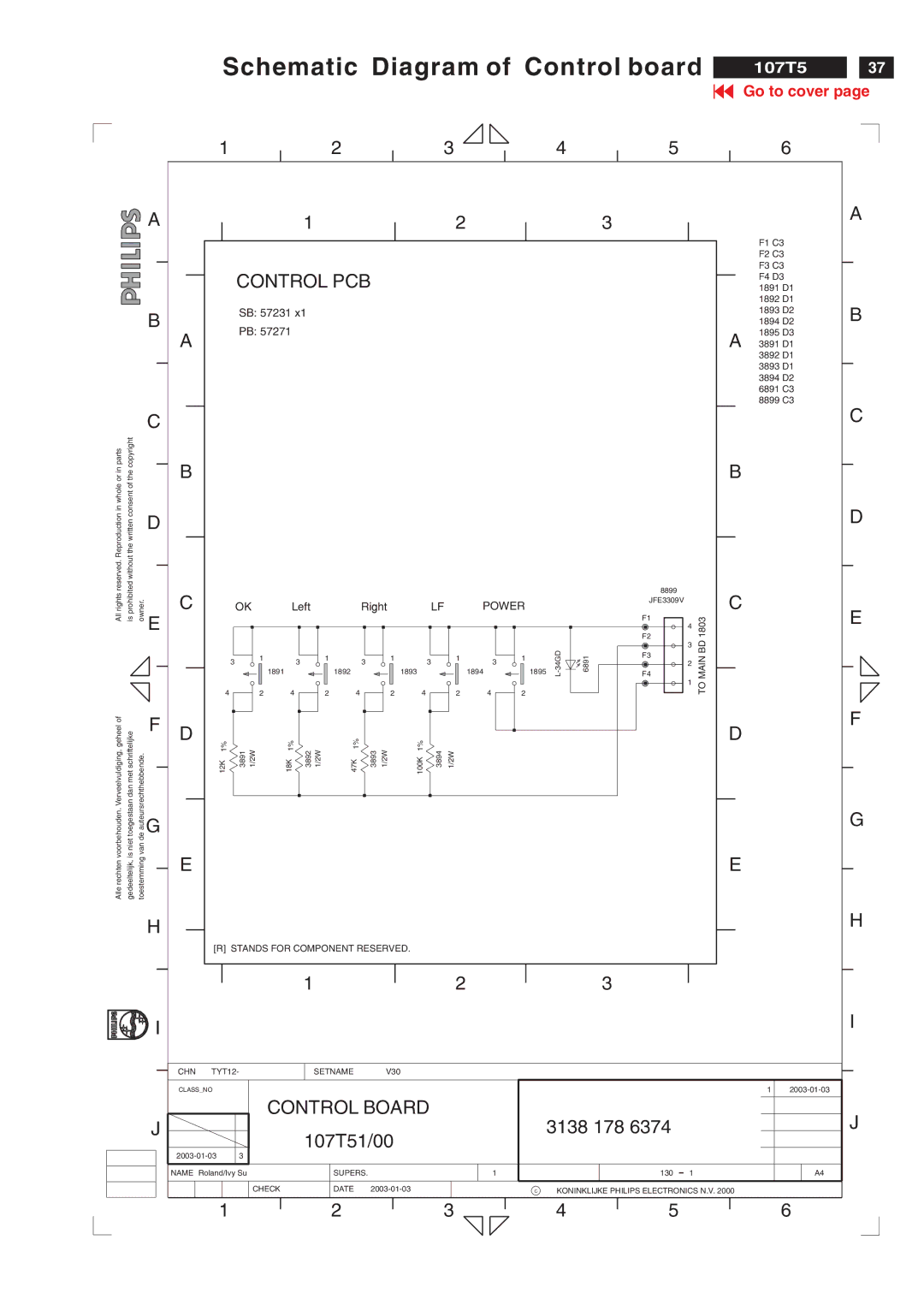
| CONTROL PCB |
|
|
|
|
|
|
|
|
|
|
| F4 D3 |
|
| ||||||
|
|
|
|
|
|
|
|
|
|
|
|
| 1891 D1 |
| ||||||||
|
|
|
|
|
|
|
|
|
|
|
|
|
|
|
|
|
|
|
| 1892 D1 |
| |
|
| SB: 57231 x1 |
|
|
|
|
|
|
|
|
|
|
|
|
|
| 1893 D2 | B | ||||
|
|
|
|
|
|
|
|
|
|
|
|
|
|
|
|
|
|
|
| 1894 D2 | ||
A |
| PB: 57271 |
|
|
|
|
|
|
|
|
|
|
|
|
|
| A | 1895 D3 |
| |||
|
|
|
|
|
|
|
|
|
|
|
|
|
|
|
|
|
| 3891 D1 |
| |||
|
|
|
|
|
|
|
|
|
|
|
|
|
|
|
|
|
|
|
| 3892 D1 |
| |
|
|
|
|
|
|
|
|
|
|
|
|
|
|
|
|
|
|
|
| 3893 D1 |
| |
|
|
|
|
|
|
|
|
|
|
|
|
|
|
|
|
|
|
|
| 3894 D2 |
| |
|
|
|
|
|
|
|
|
|
|
|
|
|
|
|
|
|
|
|
| 6891 C3 |
| |
|
|
|
|
|
|
|
|
|
|
|
|
|
|
|
|
|
|
|
| 8899 C3 |
| |
|
|
|
|
|
|
|
|
|
|
|
|
|
|
|
|
|
|
|
|
|
| C |
B |
|
|
|
|
|
|
|
|
|
|
|
|
|
|
|
|
|
| B |
|
|
|
|
|
|
|
|
|
|
|
|
|
|
|
|
|
|
|
|
|
|
|
|
| D |
|
|
|
|
|
|
|
|
|
|
|
|
|
|
|
|
| 8899 |
|
|
|
|
|
C |
| OK | Left |
|
| Right |
| LF |
| POWER |
|
| JFE3309V |
| C |
|
|
| ||||
|
|
|
|
|
|
|
|
|
|
| E | |||||||||||
|
|
|
|
|
|
|
|
|
|
|
|
|
|
|
|
| F1 |
| 1803 |
|
| |
|
|
|
|
|
|
|
|
|
|
|
|
|
|
|
|
|
| 4 |
|
| ||
|
|
|
|
|
|
|
|
|
|
|
|
|
|
|
|
|
|
|
|
| ||
|
|
|
|
|
|
|
|
|
|
|
|
|
|
|
|
| F2 |
|
|
|
| |
|
|
|
|
|
|
|
|
|
|
|
|
|
|
|
|
|
| MAINBD |
|
|
| |
|
|
|
|
|
|
|
|
|
|
|
|
|
|
|
|
| 3 |
|
|
| ||
| 3 |
| 1 |
| 3 | 1 |
| 3 | 1 | 3 |
| 1 | 3 | 1 | 6891 | F3 |
|
|
|
| ||
|
|
|
|
|
| 2 |
|
|
| |||||||||||||
|
|
|
|
|
|
|
|
|
|
|
|
|
| |||||||||
|
|
|
| 1891 |
|
| 1892 |
| 1893 |
|
|
| 1894 | 1895 | F4 | 1 |
|
|
| |||
|
|
|
|
|
|
|
|
|
|
|
|
|
|
|
|
|
| TO |
|
|
| |
| 4 |
| 2 | 4 |
| 2 | 4 |
| 2 | 4 |
| 2 | 4 | 2 |
|
|
|
|
|
|
| |
|
|
|
|
|
|
|
|
|
|
|
|
| ||||||||||
D |
|
|
|
|
|
|
|
|
|
|
|
|
|
|
|
|
|
| D |
|
| F |
1% |
|
| 1% |
|
| 1% |
|
| 1% |
|
|
|
|
|
|
|
|
|
|
| ||
| 3891 | 1/2W | 3892 | 1/2W | 3893 | 1/2W | 3894 | 1/2W |
|
|
|
|
|
|
|
|
|
| ||||
| 12K | 18K | 47K | 100K |
|
|
|
|
|
|
|
|
|
| ||||||||
|
|
|
|
|
|
|
|
|
|
|
|
|
|
|
|
|
|
|
|
|
| G |
E |
|
|
|
|
|
|
|
|
|
|
|
|
|
|
|
|
|
| E |
|
|
|
|
|
|
|
|
|
|
|
|
|
|
|
|
|
|
|
|
|
|
|
|
| H |
| [R] STANDS FOR COMPONENT RESERVED. |
|
|
|
|
|
|
|
|
|
|
|
|
| ||||||||
|
|
|
|
| 1 |
|
|
|
|
|
| 2 |
|
|
|
| 3 |
|
|
|
|
|
|
|
|
|
|
|
|
|
|
|
|
|
|
|
|
|
|
|
|
|
|
| I |
CHN | TYT12- |
|
|
| SETNAME |
| V30 |
|
|
|
|
|
|
|
|
|
|
|
|
| ||
CLASS_NO |
|
|
|
|
|
|
|
|
|
|
|
|
|
|
|
|
|
| 1 |
| ||
|
|
|
| CONTROL BOARD |
|
|
|
|
|
|
|
|
|
|
| J | ||||||
|
|
|
|
| 107T51/00 |
|
|
|
|
| 3138 178 6374 |
|
|
|
| |||||||
|
|
|
|
|
|
|
|
|
|
|
|
|
|
|
|
|
| |||||
|
|
|
|
|
|
|
|
|
|
|
|
|
|
|
|
|
|
|
| |||
NAME Roland/Ivy Su |
|
|
|
| SUPERS. |
|
|
|
| 1 |
|
|
| 130 | 1 |
|
| A4 |
| |||
|
|
| CHECK |
|
| DATE |
|
|
|
| CKONINKLIJKE PHILIPS ELECTRONICS N.V. 2000 |
|
|
| ||||||||
| 1 |
|
|
|
|
| 2 |
|
|
| 3 |
|
| 4 |
| 5 |
|
| 6 |
| ||