Unbuffered DIMM
datasheet
Rev. 1.0
DDR3L SDRAM
11.3.4 Differential Input Cross Point Voltage
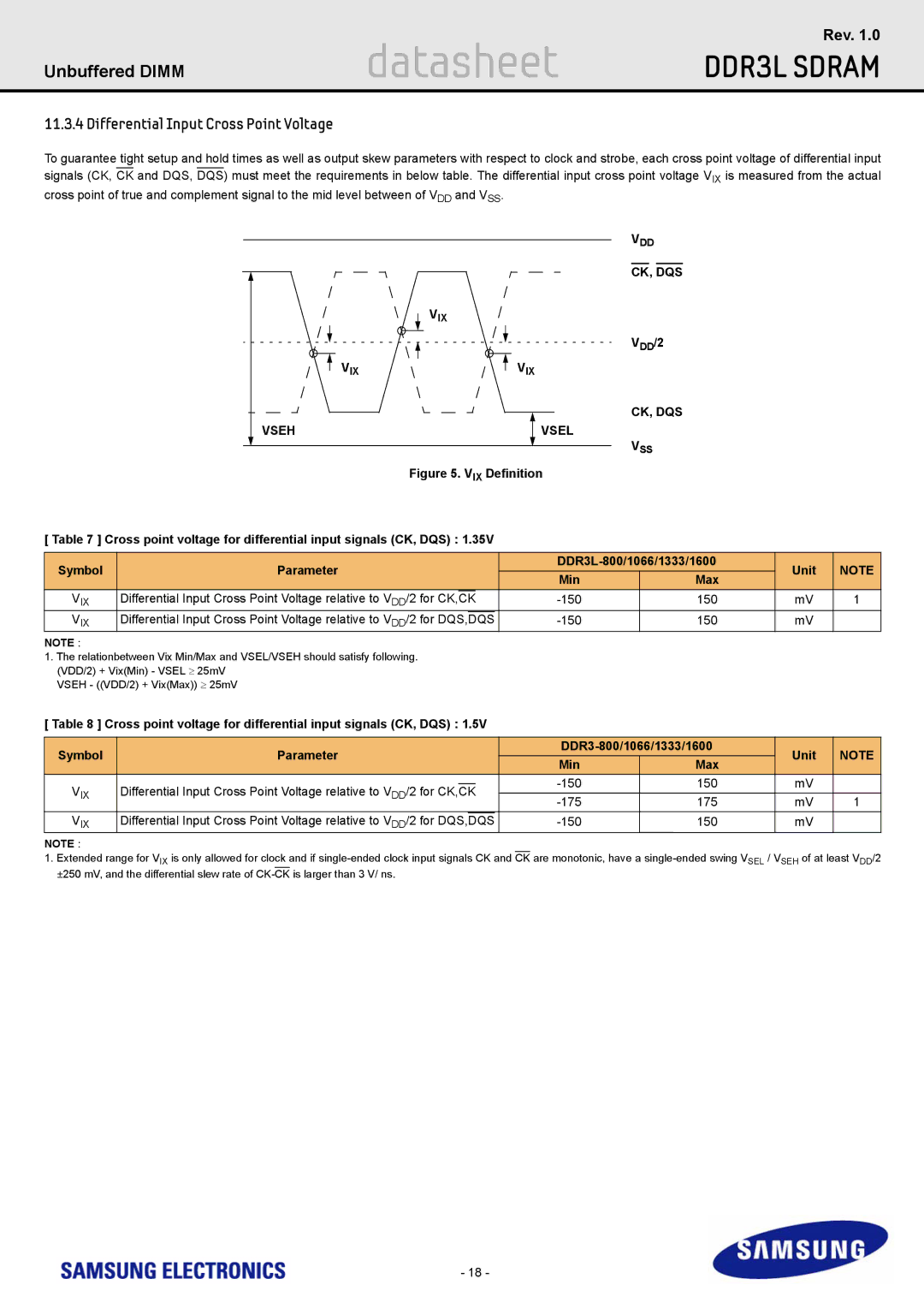
To guarantee tight setup and hold times as well as output skew parameters with respect to clock and strobe, each cross point voltage of differential input signals (CK, CK and DQS, DQS) must meet the requirements in below table. The differential input cross point voltage VIX is measured from the actual cross point of true and complement signal to the mid level between of VDD and VSS.
VDD
VIX
VIX
VSEH
CK, DQS
VDD/2
VIX
CK, DQS
VSEL
VSS
Figure 5. VIX Definition
[ Table 7 ] Cross point voltage for differential input signals (CK, DQS) : 1.35V
Symbol | Parameter |
| Unit | NOTE | |||||
Min | Max | ||||||||
|
|
|
|
|
|
| |||
VIX | Differential Input Cross Point Voltage relative to VDD/2 for CK,CK |
| 150 | mV | 1 | ||||
VIX | Differential Input Cross Point Voltage relative to VDD/2 for DQS,DQS | 150 | mV |
| |||||
NOTE :
1.The relationbetween Vix Min/Max and VSEL/VSEH should satisfy following. (VDD/2) + Vix(Min) - VSEL ≥ 25mV
VSEH - ((VDD/2) + Vix(Max)) ≥ 25mV
[ Table 8 ] Cross point voltage for differential input signals (CK, DQS) : 1.5V
Symbol | Parameter | Unit | NOTE | ||||||
Min | Max | ||||||||
|
|
|
|
|
|
| |||
VIX |
|
|
|
| 150 | mV |
| ||
Differential Input Cross Point Voltage relative to VDD/2 for CK,CK |
| ||||||||
175 | mV | 1 | |||||||
|
|
|
|
| |||||
VIX | Differential Input Cross Point Voltage relative to VDD/2 for DQS,DQS | 150 | mV |
| |||||
NOTE :
1.Extended range for VIX is only allowed for clock and if
- 18 -