Unbuffered DIMM
datasheet
Rev. 1.0
DDR3L SDRAM
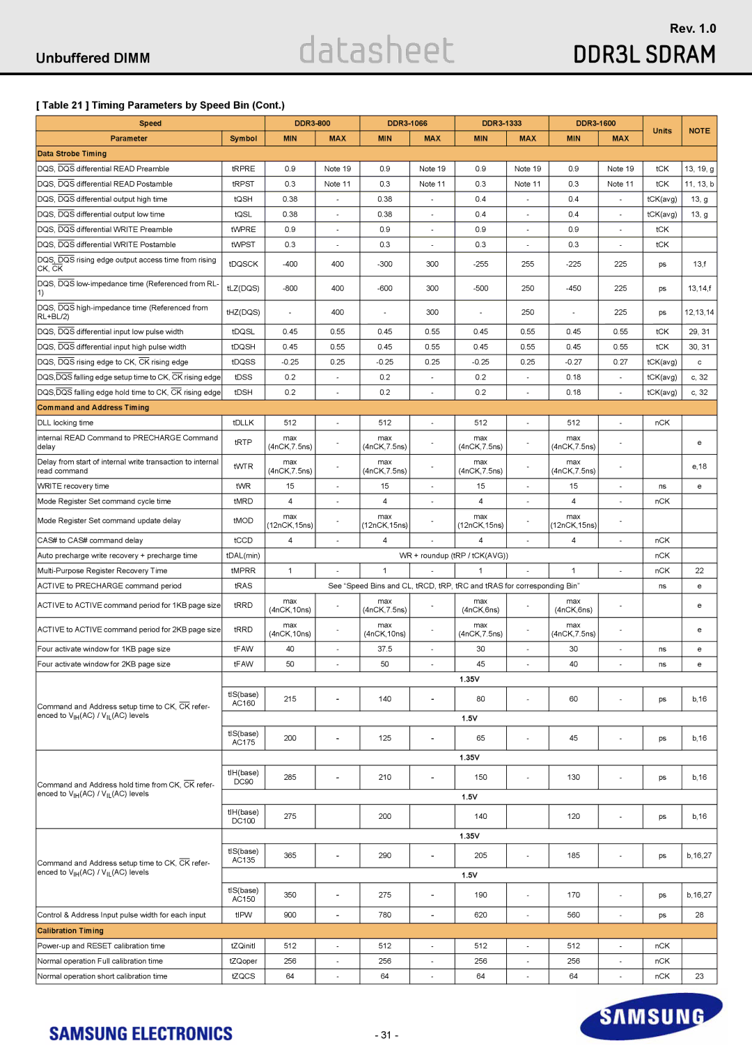
[ Table 21 ] Timing Parameters by Speed Bin (Cont.)
|
|
|
|
|
| Speed |
| Units | NOTE | |||||||||||||||||
|
|
|
|
| Parameter | Symbol | MIN | MAX | MIN | MAX | MIN |
| MAX | MIN | MAX | |||||||||||
|
|
|
|
|
|
|
| |||||||||||||||||||
Data Strobe Timing |
|
|
|
|
|
|
|
|
|
|
|
| ||||||||||||||
DQS, |
|
|
| differential READ Preamble | tRPRE | 0.9 | Note 19 | 0.9 | Note 19 | 0.9 |
| Note 19 | 0.9 | Note 19 | tCK | 13, 19, g | ||||||||||
DQS | ||||||||||||||||||||||||||
DQS, |
|
|
| differential READ Postamble | tRPST | 0.3 | Note 11 | 0.3 | Note 11 | 0.3 |
| Note 11 | 0.3 | Note 11 | tCK | 11, 13, b | ||||||||||
DQS | ||||||||||||||||||||||||||
DQS, |
|
|
| differential output high time | tQSH | 0.38 | - | 0.38 | - | 0.4 |
| - | 0.4 | - | tCK(avg) | 13, g | ||||||||||
DQS | ||||||||||||||||||||||||||
DQS, |
|
|
| differential output low time | tQSL | 0.38 | - | 0.38 | - | 0.4 |
| - | 0.4 | - | tCK(avg) | 13, g | ||||||||||
DQS | ||||||||||||||||||||||||||
DQS, |
|
|
| differential WRITE Preamble | tWPRE | 0.9 | - | 0.9 | - | 0.9 |
| - | 0.9 | - | tCK |
| ||||||||||
DQS |
| |||||||||||||||||||||||||
DQS, |
|
|
| differential WRITE Postamble | tWPST | 0.3 | - | 0.3 | - | 0.3 |
| - | 0.3 | - | tCK |
| ||||||||||
DQS |
| |||||||||||||||||||||||||
DQS, |
|
|
| rising edge output access time from rising |
|
|
|
|
|
|
|
|
|
|
|
| ||||||||||
DQS | tDQSCK | 400 | 300 |
| 255 | 225 | ps | 13,f | ||||||||||||||||||
CK, CK |
| |||||||||||||||||||||||||
|
|
|
|
|
|
|
|
|
|
|
| |||||||||||||||
|
|
|
|
|
|
|
|
|
|
|
|
|
|
|
| |||||||||||
DQS, |
|
|
|
|
|
|
|
|
|
|
|
|
|
| ||||||||||||
DQS | tLZ(DQS) | 400 | 300 |
| 250 | 225 | ps | 13,14,f | ||||||||||||||||||
1) |
|
|
|
|
|
|
|
|
|
|
|
|
|
|
| |||||||||||
|
|
|
|
|
|
|
|
|
|
|
|
|
|
|
|
|
|
|
|
|
|
|
|
|
| |
|
|
|
|
|
|
|
|
|
|
|
|
|
|
|
| |||||||||||
DQS, |
|
|
|
|
|
|
|
|
|
|
|
|
|
| ||||||||||||
DQS | tHZ(DQS) | - | 400 | - | 300 | - |
| 250 | - | 225 | ps | 12,13,14 | ||||||||||||||
RL+BL/2) |
| |||||||||||||||||||||||||
|
|
|
|
|
|
|
|
|
|
|
| |||||||||||||||
|
|
|
|
|
|
|
|
|
|
|
|
|
|
|
| |||||||||||
DQS, |
|
| differential input low pulse width | tDQSL | 0.45 | 0.55 | 0.45 | 0.55 | 0.45 |
| 0.55 | 0.45 | 0.55 | tCK | 29, 31 | |||||||||||
DQS | ||||||||||||||||||||||||||
DQS, |
|
|
| differential input high pulse width | tDQSH | 0.45 | 0.55 | 0.45 | 0.55 | 0.45 |
| 0.55 | 0.45 | 0.55 | tCK | 30, 31 | ||||||||||
DQS | ||||||||||||||||||||||||||
DQS, |
|
|
| rising edge to CK, |
| rising edge | tDQSS | 0.25 | 0.25 |
| 0.25 | 0.27 | tCK(avg) | c | ||||||||||||
DQS | CK | |||||||||||||||||||||||||
|
|
| falling edge setup time to CK, |
|
|
| rising edge | tDSS | 0.2 | - | 0.2 | - | 0.2 |
| - | 0.18 | - | tCK(avg) | c, 32 | |||||||
DQS,DQS | CK | |||||||||||||||||||||||||
|
|
| falling edge hold time to CK, |
|
|
| rising edge | tDSH | 0.2 | - | 0.2 | - | 0.2 |
| - | 0.18 | - | tCK(avg) | c, 32 | |||||||
DQS,DQS | CK | |||||||||||||||||||||||||
Command and Address Timing |
|
|
|
|
|
|
|
|
|
|
|
| ||||||||||||||
DLL locking time | tDLLK | 512 | - | 512 | - | 512 |
| - | 512 | - | nCK |
| ||||||||||||||
|
|
|
|
|
|
|
|
|
|
|
|
| ||||||||||||||
internal READ Command to PRECHARGE Command | tRTP | max | - | max | - | max |
| - | max | - |
| e | ||||||||||||||
delay | (4nCK,7.5ns) | (4nCK,7.5ns) | (4nCK,7.5ns) |
| (4nCK,7.5ns) |
| ||||||||||||||||||||
|
|
|
|
|
|
|
| |||||||||||||||||||
|
|
|
|
|
|
|
|
|
|
|
|
| ||||||||||||||
Delay from start of internal write transaction to internal | tWTR | max | - | max | - | max |
| - | max | - |
| e,18 | ||||||||||||||
read command | (4nCK,7.5ns) | (4nCK,7.5ns) | (4nCK,7.5ns) |
| (4nCK,7.5ns) |
| ||||||||||||||||||||
|
|
|
|
|
|
|
| |||||||||||||||||||
|
|
|
|
|
|
|
|
|
|
|
|
| ||||||||||||||
WRITE recovery time | tWR | 15 | - | 15 | - | 15 |
| - | 15 | - | ns | e | ||||||||||||||
|
|
|
|
|
|
|
|
|
|
|
|
| ||||||||||||||
Mode Register Set command cycle time | tMRD | 4 | - | 4 | - | 4 |
| - | 4 | - | nCK |
| ||||||||||||||
|
|
|
|
|
|
|
|
|
|
|
|
|
|
|
|
|
|
|
|
|
|
|
|
|
|
|
Mode Register Set command update delay | tMOD | max | - | max | - | max |
| - | max | - |
|
| ||||||||||||||
(12nCK,15ns) | (12nCK,15ns) | (12nCK,15ns) |
| (12nCK,15ns) |
|
| ||||||||||||||||||||
|
|
|
|
|
|
|
|
|
|
|
|
|
|
|
|
|
|
|
|
|
|
| ||||
|
|
|
|
|
|
|
|
|
|
|
|
| ||||||||||||||
CAS# to CAS# command delay | tCCD | 4 | - | 4 | - | 4 |
| - | 4 | - | nCK |
| ||||||||||||||
|
|
|
|
|
|
|
|
|
|
|
|
| ||||||||||||||
Auto precharge write recovery + precharge time | tDAL(min) |
|
| WR + roundup (tRP / tCK(AVG)) |
|
|
| nCK |
| |||||||||||||||||
|
|
|
|
|
|
|
|
|
|
|
|
| ||||||||||||||
tMPRR | 1 | - | 1 | - | 1 |
| - | 1 | - | nCK | 22 | |||||||||||||||
|
|
|
|
|
|
|
|
|
|
|
| |||||||||||||||
ACTIVE to PRECHARGE command period | tRAS |
| See “Speed Bins and CL, tRCD, tRP, tRC and tRAS for corresponding Bin” |
| ns | e | ||||||||||||||||||||
|
|
|
|
|
|
|
|
|
|
|
|
|
|
|
|
|
|
|
|
|
|
|
|
|
|
|
ACTIVE to ACTIVE command period for 1KB page size | tRRD | max | - | max | - | max |
| - | max | - |
| e | ||||||||||||||
(4nCK,10ns) | (4nCK,7.5ns) | (4nCK,6ns) |
| (4nCK,6ns) |
| |||||||||||||||||||||
|
|
|
|
|
|
|
|
|
|
|
|
|
|
|
|
|
|
|
|
|
|
| ||||
|
|
|
|
|
|
|
|
|
|
|
|
|
|
|
|
|
|
|
|
|
|
|
|
|
|
|
ACTIVE to ACTIVE command period for 2KB page size | tRRD | max | - | max | - | max |
| - | max | - |
| e | ||||||||||||||
(4nCK,10ns) | (4nCK,10ns) | (4nCK,7.5ns) |
| (4nCK,7.5ns) |
| |||||||||||||||||||||
|
|
|
|
|
|
|
|
|
|
|
|
|
|
|
|
|
|
|
|
|
|
| ||||
|
|
|
|
|
|
|
|
|
|
|
|
| ||||||||||||||
Four activate window for 1KB page size | tFAW | 40 | - | 37.5 | - | 30 |
| - | 30 | - | ns | e | ||||||||||||||
|
|
|
|
|
|
|
|
|
|
|
|
| ||||||||||||||
Four activate window for 2KB page size | tFAW | 50 | - | 50 | - | 45 |
| - | 40 | - | ns | e | ||||||||||||||
|
|
|
|
|
|
|
|
|
|
|
|
|
|
|
|
|
|
|
|
|
|
|
|
|
|
|
|
|
|
|
|
|
|
|
|
|
|
|
|
|
|
|
|
|
|
| 1.35V |
|
|
|
|
| |
|
|
|
|
|
|
|
|
|
|
|
|
|
|
|
|
|
|
|
|
|
|
|
|
|
|
|
|
|
|
|
|
|
|
|
|
|
|
|
|
|
| tIS(base) | 215 | - | 140 | - | 80 |
| - | 60 | - | ps | b,16 |
|
|
|
|
|
|
|
|
|
|
|
|
|
|
| AC160 |
| ||||||||||
Command and Address setup time to CK, CK refer- |
|
|
|
|
|
|
|
|
|
|
| |||||||||||||||
|
|
|
|
|
|
|
|
|
|
|
| |||||||||||||||
enced to VIH(AC) / VIL(AC) levels |
|
|
|
|
| 1.5V |
|
|
|
|
| |||||||||||||||
|
|
|
|
|
|
|
|
|
|
|
|
|
|
| tIS(base) | 200 | - | 125 | - | 65 |
| - | 45 | - | ps | b,16 |
|
|
|
|
|
|
|
|
|
|
|
|
|
|
| AC175 |
| ||||||||||
|
|
|
|
|
|
|
|
|
|
|
|
|
|
|
|
|
|
|
|
|
|
|
|
|
| |
|
|
|
|
|
|
|
|
|
|
|
|
|
|
|
|
|
|
|
|
|
|
|
|
|
|
|
|
|
|
|
|
|
|
|
|
|
|
|
|
|
|
|
|
|
|
| 1.35V |
|
|
|
|
| |
|
|
|
|
|
|
|
|
|
|
|
|
|
|
|
|
|
|
|
|
|
|
|
|
|
|
|
|
|
|
|
|
|
|
|
|
|
|
|
|
|
| tIH(base) | 285 | - | 210 | - | 150 |
| - | 130 | - | ps | b,16 |
|
|
|
|
|
|
|
|
|
|
|
|
|
|
| DC90 |
| ||||||||||
Command and Address hold time from CK, CK refer- |
|
|
|
|
|
|
|
|
|
|
| |||||||||||||||
|
|
|
|
|
|
|
|
|
|
|
| |||||||||||||||
enced to VIH(AC) / VIL(AC) levels |
|
|
|
|
| 1.5V |
|
|
|
|
| |||||||||||||||
|
|
|
|
|
|
|
|
|
|
|
|
|
|
| tIH(base) | 275 |
| 200 |
| 140 |
|
| 120 | - | ps | b,16 |
|
|
|
|
|
|
|
|
|
|
|
|
|
|
| DC100 |
|
|
|
| |||||||
|
|
|
|
|
|
|
|
|
|
|
|
|
|
|
|
|
|
|
|
|
|
|
|
|
| |
|
|
|
|
|
|
|
|
|
|
|
|
|
|
|
|
|
|
|
|
|
|
|
|
|
|
|
|
|
|
|
|
|
|
|
|
|
|
|
|
|
|
|
|
|
|
| 1.35V |
|
|
|
|
| |
|
|
|
|
|
|
|
|
|
|
|
|
|
|
|
|
|
|
|
|
|
|
|
|
|
|
|
|
|
|
|
|
|
|
|
|
|
|
|
|
|
| tIS(base) | 365 | - | 290 | - | 205 |
| - | 185 | - | ps | b,16,27 |
|
|
|
|
|
|
|
|
|
|
|
|
|
|
| AC135 |
| ||||||||||
Command and Address setup time to CK, CK refer- |
|
|
|
|
|
|
|
|
|
|
| |||||||||||||||
|
|
|
|
|
|
|
|
|
|
|
| |||||||||||||||
enced to VIH(AC) / VIL(AC) levels |
|
|
|
|
| 1.5V |
|
|
|
|
| |||||||||||||||
|
|
|
|
|
|
|
|
|
|
|
|
|
|
| tIS(base) | 350 | - | 275 | - | 190 |
| - | 170 | - | ps | b,16,27 |
|
|
|
|
|
|
|
|
|
|
|
|
|
|
| AC150 |
| ||||||||||
|
|
|
|
|
|
|
|
|
|
|
|
|
|
|
|
|
|
|
|
|
|
|
|
|
| |
|
|
|
|
|
|
|
|
|
|
|
|
| ||||||||||||||
Control & Address Input pulse width for each input | tIPW | 900 | - | 780 | - | 620 |
| - | 560 | - | ps | 28 | ||||||||||||||
|
|
|
|
|
|
|
|
|
|
|
|
| ||||||||||||||
Calibration Timing |
|
|
|
|
|
|
|
|
|
|
|
| ||||||||||||||
tZQinitI | 512 | - | 512 | - | 512 |
| - | 512 | - | nCK |
| |||||||||||||||
|
|
|
|
|
|
|
|
|
|
|
|
| ||||||||||||||
Normal operation Full calibration time | tZQoper | 256 | - | 256 | - | 256 |
| - | 256 | - | nCK |
| ||||||||||||||
|
|
|
|
|
|
|
|
|
|
|
|
| ||||||||||||||
Normal operation short calibration time | tZQCS | 64 | - | 64 | - | 64 |
| - | 64 | - | nCK | 23 | ||||||||||||||
|
|
|
|
|
|
|
|
|
|
|
|
|
|
|
|
|
|
|
|
|
|
|
|
|
|
|
- 31 -