Unbuffered DIMM
datasheet
Rev. 1.0
DDR3L SDRAM
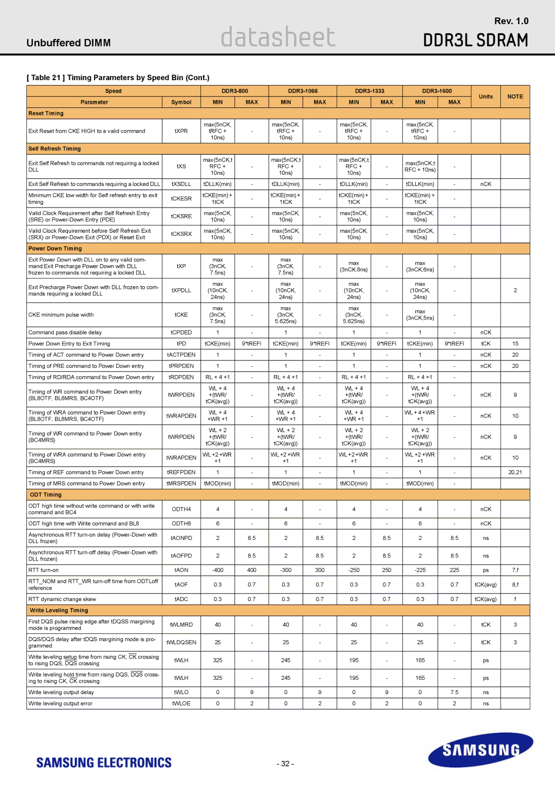
[ Table 21 ] Timing Parameters by Speed Bin (Cont.)
Speed |
| Units | NOTE | |||||||||||||
Parameter | Symbol | MIN | MAX | MIN | MAX | MIN | MAX | MIN | MAX | |||||||
|
| |||||||||||||||
Reset Timing |
|
|
|
|
|
|
|
|
|
|
| |||||
|
|
|
|
|
| max(5nCK, |
| max(5nCK, |
| max(5nCK, |
| max(5nCK, |
|
|
| |
Exit Reset from CKE HIGH to a valid command | tXPR | tRFC + | - | tRFC + | - | tRFC + | - | tRFC + | - |
|
| |||||
|
|
|
|
|
| 10ns) |
| 10ns) |
| 10ns) |
| 10ns) |
|
|
| |
|
|
|
|
|
|
|
|
|
|
|
|
|
|
|
| |
Self Refresh Timing |
|
|
|
|
|
|
|
|
|
|
| |||||
Exit Self Refresh to commands not requiring a locked |
| max(5nCK,t |
| max(5nCK,t |
| max(5nCK,t |
| max(5nCK,t |
|
|
| |||||
tXS | RFC + | - | RFC + | - | RFC + | - | - |
|
| |||||||
DLL | RFC + 10ns) |
|
| |||||||||||||
| 10ns) |
| 10ns) |
| 10ns) |
|
|
|
| |||||||
|
|
|
|
|
|
|
|
|
|
|
|
| ||||
|
|
|
|
|
|
|
|
|
|
|
| |||||
Exit Self Refresh to commands requiring a locked DLL | tXSDLL | tDLLK(min) | - | tDLLK(min) | - | tDLLK(min) | - | tDLLK(min) | - | nCK |
| |||||
|
|
|
|
|
|
|
|
|
|
|
| |||||
Minimum CKE low width for Self refresh entry to exit | tCKESR | tCKE(min) + | - | tCKE(min)+ | - | tCKE(min) + | - | tCKE(min) + | - |
|
| |||||
timing | 1tCK | 1tCK | 1tCK | 1tCK |
|
| ||||||||||
|
|
|
|
|
|
| ||||||||||
|
|
|
|
|
|
|
|
|
|
|
| |||||
Valid Clock Requirement after Self Refresh Entry | tCKSRE | max(5nCK, | - | max(5nCK, | - | max(5nCK, | - | max(5nCK, | - |
|
| |||||
(SRE) or | 10ns) | 10ns) | 10ns) | 10ns) |
|
| ||||||||||
|
|
|
|
|
|
| ||||||||||
|
|
|
|
|
|
|
|
|
|
|
| |||||
Valid Clock Requirement before Self Refresh Exit | tCKSRX | max(5nCK, | - | max(5nCK, | - | max(5nCK, | - | max(5nCK, | - |
|
| |||||
(SRX) or | 10ns) | 10ns) | 10ns) | 10ns) |
|
| ||||||||||
|
|
|
|
|
|
| ||||||||||
|
|
|
|
|
|
|
|
|
|
|
|
|
|
|
| |
Power Down Timing |
|
|
|
|
|
|
|
|
|
|
| |||||
Exit Power Down with DLL on to any valid com- | tXP | max | - | max | - | max | - | max | - |
|
| |||||
mand;Exit Precharge Power Down with DLL | (3nCK, | (3nCK, |
|
| ||||||||||||
(3nCK,6ns) | (3nCK,6ns) |
|
| |||||||||||||
frozen to commands not requiring a locked DLL |
| 7.5ns) |
| 7.5ns) |
|
|
|
|
| |||||||
|
|
|
|
|
|
|
|
| ||||||||
|
|
|
|
|
|
|
|
|
|
|
|
|
|
|
| |
Exit Precharge Power Down with DLL frozen to com- |
| max |
| max |
| max |
| max |
|
|
| |||||
tXPDLL | (10nCK, | - | (10nCK, | - | (10nCK, | - | (10nCK, | - |
| 2 | ||||||
mands requiring a locked DLL |
| |||||||||||||||
| 24ns) |
| 24ns) |
| 24ns) |
| 24ns) |
|
|
| ||||||
|
|
|
|
|
|
|
|
|
|
|
| |||||
|
|
|
|
|
|
|
|
|
|
|
|
|
|
|
| |
|
|
|
|
|
| max |
| max |
| max |
| max |
|
|
| |
CKE minimum pulse width | tCKE | (3nCK, | - | (3nCK, | - | (3nCK, | - | - |
|
| ||||||
(3nCK,5ns) |
|
| ||||||||||||||
|
|
|
|
|
| 7.5ns) |
| 5.625ns) |
| 5.625ns) |
|
|
|
| ||
|
|
|
|
|
|
|
|
|
|
|
|
| ||||
|
|
|
|
|
|
|
|
|
|
|
| |||||
Command pass disable delay | tCPDED | 1 | - | 1 | - | 1 | - | 1 | - | nCK |
| |||||
|
|
|
|
|
|
|
|
|
|
|
| |||||
Power Down Entry to Exit Timing | tPD | tCKE(min) | 9*tREFI | tCKE(min) | 9*tREFI | tCKE(min) | 9*tREFI | tCKE(min) | 9*tREFI | tCK | 15 | |||||
|
|
|
|
|
|
|
|
|
|
|
| |||||
Timing of ACT command to Power Down entry | tACTPDEN | 1 | - | 1 | - | 1 | - | 1 | - | nCK | 20 | |||||
|
|
|
|
|
|
|
|
|
|
|
| |||||
Timing of PRE command to Power Down entry | tPRPDEN | 1 | - | 1 | - | 1 | - | 1 | - | nCK | 20 | |||||
|
|
|
|
|
|
|
|
|
|
|
| |||||
Timing of RD/RDA command to Power Down entry | tRDPDEN | RL + 4 +1 | - | RL + 4 +1 | - | RL + 4 +1 | - | RL + 4 +1 | - |
|
| |||||
|
|
|
|
|
|
|
|
|
|
|
|
|
|
|
| |
Timing of WR command to Power Down entry |
| WL + 4 |
| WL + 4 |
| WL + 4 |
| WL + 4 |
|
|
| |||||
tWRPDEN | +(tWR/ | - | +(tWR/ | - | +(tWR/ | - | +(tWR/ | - | nCK | 9 | ||||||
(BL8OTF, BL8MRS, BC4OTF) | ||||||||||||||||
| tCK(avg)) |
| tCK(avg)) |
| tCK(avg)) |
| tCK(avg)) |
|
|
| ||||||
|
|
|
|
|
|
|
|
|
|
|
| |||||
|
|
|
|
|
|
|
|
|
|
|
| |||||
Timing of WRA command to Power Down entry | tWRAPDEN | WL + 4 | - | WL + 4 | - | WL + 4 | - | WL + 4 +WR | - | nCK | 10 | |||||
(BL8OTF, BL8MRS, BC4OTF) | +WR +1 | +WR +1 | +WR +1 | +1 | ||||||||||||
|
|
|
|
|
|
| ||||||||||
|
|
|
|
|
|
|
|
|
|
|
|
|
|
|
| |
Timing of WR command to Power Down entry |
| WL + 2 |
| WL + 2 |
| WL + 2 |
| WL + 2 |
|
|
| |||||
tWRPDEN | +(tWR/ | - | +(tWR/ | - | +(tWR/ | - | +(tWR/ | - | nCK | 9 | ||||||
(BC4MRS) | ||||||||||||||||
| tCK(avg)) |
| tCK(avg)) |
| tCK(avg)) |
| tCK(avg)) |
|
|
| ||||||
|
|
|
|
|
|
|
|
|
|
|
| |||||
|
|
|
|
|
|
|
|
|
|
|
| |||||
Timing of WRA command to Power Down entry | tWRAPDEN | WL +2 +WR | - | WL +2 +WR | - | WL +2 +WR | - | WL +2 +WR | - | nCK | 10 | |||||
(BC4MRS) | +1 | +1 | +1 | +1 | ||||||||||||
|
|
|
|
|
|
| ||||||||||
|
|
|
|
|
|
|
|
|
|
|
| |||||
Timing of REF command to Power Down entry | tREFPDEN | 1 | - | 1 | - | 1 | - | 1 | - |
| 20,21 | |||||
|
|
|
|
|
|
|
|
|
|
|
| |||||
Timing of MRS command to Power Down entry | tMRSPDEN | tMOD(min) | - | tMOD(min) | - | tMOD(min) | - | tMOD(min) | - |
|
| |||||
|
|
|
|
|
|
|
|
|
|
|
|
|
|
|
| |
ODT Timing |
|
|
|
|
|
|
|
|
|
|
| |||||
ODT high time without write command or with write | ODTH4 | 4 | - | 4 | - | 4 | - | 4 | - | nCK |
| |||||
command and BC4 |
| |||||||||||||||
|
|
|
|
|
|
|
|
|
|
| ||||||
|
|
|
|
|
|
|
|
|
|
|
| |||||
ODT high time with Write command and BL8 | ODTH8 | 6 | - | 6 | - | 6 | - | 6 | - | nCK |
| |||||
|
|
|
|
|
|
|
|
|
|
|
| |||||
Asynchronous RTT | tAONPD | 2 | 8.5 | 2 | 8.5 | 2 | 8.5 | 2 | 8.5 | ns |
| |||||
DLL frozen) |
| |||||||||||||||
|
|
|
|
|
|
|
|
|
|
| ||||||
|
|
|
|
|
|
|
|
|
|
|
| |||||
Asynchronous RTT | tAOFPD | 2 | 8.5 | 2 | 8.5 | 2 | 8.5 | 2 | 8.5 | ns |
| |||||
DLL frozen) |
| |||||||||||||||
|
|
|
|
|
|
|
|
|
|
| ||||||
|
|
|
|
|
|
|
|
|
|
|
| |||||
RTT | tAON | 400 | 300 | 250 | 225 | ps | 7,f | |||||||||
|
|
|
|
|
|
|
|
|
|
|
| |||||
RTT_NOM and RTT_WR | tAOF | 0.3 | 0.7 | 0.3 | 0.7 | 0.3 | 0.7 | 0.3 | 0.7 | tCK(avg) | 8,f | |||||
reference | ||||||||||||||||
|
|
|
|
|
|
|
|
|
|
| ||||||
|
|
|
|
|
|
|
|
|
|
|
| |||||
RTT dynamic change skew | tADC | 0.3 | 0.7 | 0.3 | 0.7 | 0.3 | 0.7 | 0.3 | 0.7 | tCK(avg) | f | |||||
|
|
|
|
|
|
|
|
|
|
|
|
|
|
|
| |
Write Leveling Timing |
|
|
|
|
|
|
|
|
|
|
| |||||
First DQS pulse rising edge after tDQSS margining | tWLMRD | 40 | - | 40 | - | 40 | - | 40 | - | tCK | 3 | |||||
mode is programmed | ||||||||||||||||
|
|
|
|
|
|
|
|
|
|
| ||||||
|
|
|
|
|
|
|
|
|
|
|
| |||||
DQS/DQS delay after tDQS margining mode is pro- | tWLDQSEN | 25 | - | 25 | - | 25 | - | 25 | - | tCK | 3 | |||||
grammed | ||||||||||||||||
|
|
|
|
|
|
|
|
|
|
| ||||||
|
|
|
|
|
|
|
|
|
|
|
|
|
|
| ||
Write leveling setup time from rising CK, |
|
| crossing |
|
|
|
|
|
|
|
|
|
|
| ||
CK | tWLH | 325 | - | 245 | - | 195 | - | 165 | - | ps |
| |||||
to rising DQS, DQS crossing |
| |||||||||||||||
|
|
|
|
|
|
|
|
|
|
| ||||||
|
|
|
|
|
|
|
|
|
|
|
|
|
| |||
Write leveling hold time from rising DQS, |
|
| cross- |
|
|
|
|
|
|
|
|
|
|
| ||
DQS | tWLH | 325 | - | 245 | - | 195 | - | 165 | - | ps |
| |||||
ing to rising CK, CK crossing |
| |||||||||||||||
|
|
|
|
|
|
|
|
|
|
| ||||||
|
|
|
|
|
|
|
|
|
|
|
| |||||
Write leveling output delay | tWLO | 0 | 9 | 0 | 9 | 0 | 9 | 0 | 7.5 | ns |
| |||||
|
|
|
|
|
|
|
|
|
|
|
| |||||
Write leveling output error | tWLOE | 0 | 2 | 0 | 2 | 0 | 2 | 0 | 2 | ns |
| |||||
|
|
|
|
|
|
|
|
|
|
|
|
|
|
|
| |
- 32 -