Unbuffered DIMM
datasheet
Rev. 1.0
DDR3L SDRAM
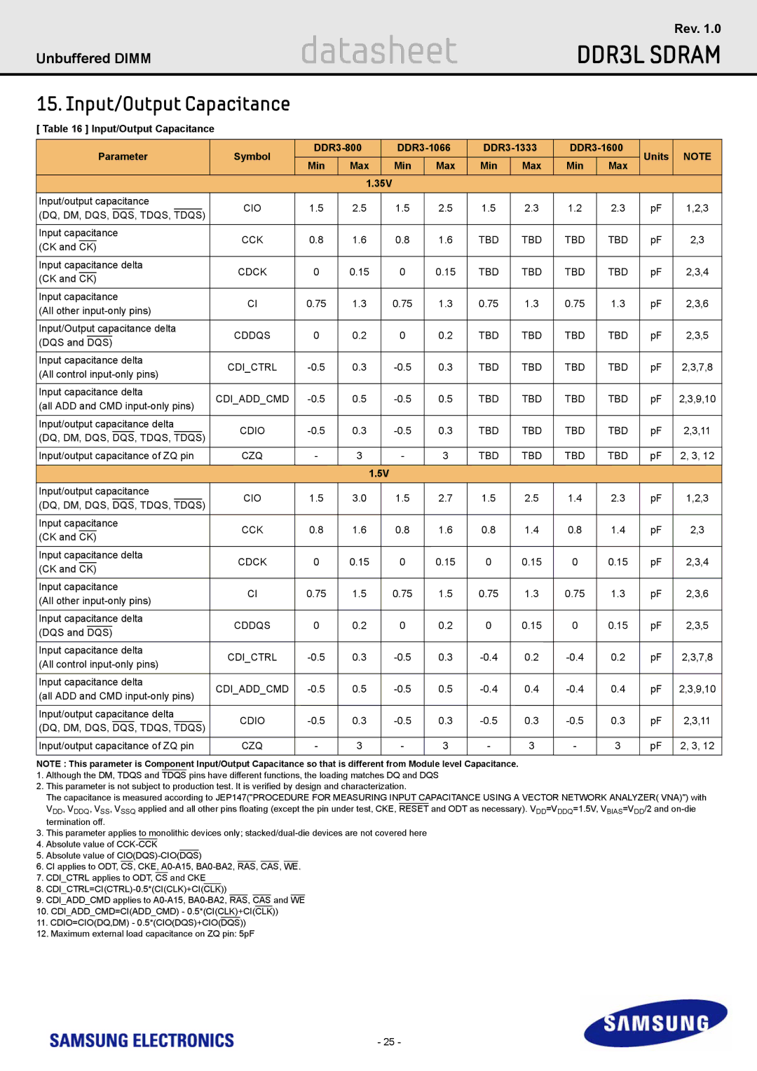
15. Input/Output Capacitance
[ Table 16 ] Input/Output Capacitance
|
|
| Parameter | Symbol |
| Units | NOTE | |||||||||||||
|
|
| Min | Max |
| Min | Max | Min | Max | Min | Max | |||||||||
|
|
|
|
|
|
|
|
|
|
|
| |||||||||
|
|
|
|
|
|
|
|
|
| 1.35V |
|
|
|
|
|
|
|
| ||
Input/output capacitance | CIO | 1.5 | 2.5 |
| 1.5 | 2.5 | 1.5 | 2.3 | 1.2 | 2.3 | pF | 1,2,3 | ||||||||
|
|
|
|
|
|
|
|
| ||||||||||||
(DQ, DM, DQS, DQS, TDQS, TDQS) | ||||||||||||||||||||
|
|
|
|
|
|
|
|
|
|
|
| |||||||||
|
|
|
|
|
|
|
|
|
|
|
|
| ||||||||
Input capacitance | CCK | 0.8 | 1.6 |
| 0.8 | 1.6 | TBD | TBD | TBD | TBD | pF | 2,3 | ||||||||
|
|
|
|
|
|
|
|
| ||||||||||||
(CK and CK) | ||||||||||||||||||||
|
|
|
|
|
|
|
|
|
|
|
| |||||||||
|
|
|
|
|
|
|
|
|
|
|
|
| ||||||||
Input capacitance delta | CDCK | 0 | 0.15 |
| 0 | 0.15 | TBD | TBD | TBD | TBD | pF | 2,3,4 | ||||||||
|
|
|
|
|
|
|
|
| ||||||||||||
(CK and CK) | ||||||||||||||||||||
|
|
|
|
|
|
|
|
|
|
|
| |||||||||
Input capacitance | CI | 0.75 | 1.3 |
| 0.75 | 1.3 | 0.75 | 1.3 | 0.75 | 1.3 | pF | 2,3,6 | ||||||||
(All other |
| |||||||||||||||||||
|
|
|
|
|
|
|
|
|
|
|
| |||||||||
|
|
|
|
|
|
|
|
|
|
|
|
| ||||||||
Input/Output capacitance delta | CDDQS | 0 | 0.2 |
| 0 | 0.2 | TBD | TBD | TBD | TBD | pF | 2,3,5 | ||||||||
|
|
|
|
|
|
|
|
| ||||||||||||
(DQS and DQS) | ||||||||||||||||||||
|
|
|
|
|
|
|
|
|
|
|
| |||||||||
|
|
|
|
|
|
|
|
|
|
|
|
| ||||||||
Input capacitance delta | CDI_CTRL | 0.3 |
| 0.3 | TBD | TBD | TBD | TBD | pF | 2,3,7,8 | ||||||||||
(All control |
| |||||||||||||||||||
|
|
|
|
|
|
|
|
|
|
|
| |||||||||
|
|
|
|
|
|
|
|
|
|
|
|
| ||||||||
Input capacitance delta | CDI_ADD_CMD | 0.5 |
| 0.5 | TBD | TBD | TBD | TBD | pF | 2,3,9,10 | ||||||||||
(all ADD and CMD |
| |||||||||||||||||||
|
|
|
|
|
|
|
|
|
|
|
| |||||||||
|
|
|
|
|
|
|
|
|
|
|
|
| ||||||||
Input/output capacitance delta | CDIO | 0.3 |
| 0.3 | TBD | TBD | TBD | TBD | pF | 2,3,11 | ||||||||||
|
|
|
|
|
|
|
|
| ||||||||||||
(DQ, DM, DQS, DQS, TDQS, TDQS) | ||||||||||||||||||||
|
|
|
|
|
|
|
|
|
|
|
| |||||||||
|
|
|
|
|
|
|
|
|
|
|
|
| ||||||||
Input/output capacitance of ZQ pin | CZQ | - | 3 |
| - | 3 | TBD | TBD | TBD | TBD | pF | 2, 3, 12 | ||||||||
|
|
|
|
|
|
|
|
|
|
|
|
|
|
|
|
|
|
|
| |
|
|
|
|
|
|
|
|
|
| 1.5V |
|
|
|
|
|
|
|
| ||
Input/output capacitance | CIO | 1.5 | 3.0 |
| 1.5 | 2.7 | 1.5 | 2.5 | 1.4 | 2.3 | pF | 1,2,3 | ||||||||
|
|
|
|
|
|
|
|
| ||||||||||||
(DQ, DM, DQS, DQS, TDQS, TDQS) | ||||||||||||||||||||
|
|
|
|
|
|
|
|
|
|
|
| |||||||||
|
|
|
|
|
|
|
|
|
|
|
|
| ||||||||
Input capacitance | CCK | 0.8 | 1.6 |
| 0.8 | 1.6 | 0.8 | 1.4 | 0.8 | 1.4 | pF | 2,3 | ||||||||
|
|
|
|
|
|
|
|
| ||||||||||||
(CK and CK) | ||||||||||||||||||||
|
|
|
|
|
|
|
|
|
|
|
| |||||||||
|
|
|
|
|
|
|
|
|
|
|
|
| ||||||||
Input capacitance delta | CDCK | 0 | 0.15 |
| 0 | 0.15 | 0 | 0.15 | 0 | 0.15 | pF | 2,3,4 | ||||||||
|
|
|
|
|
|
|
|
| ||||||||||||
(CK and CK) | ||||||||||||||||||||
|
|
|
|
|
|
|
|
|
|
|
| |||||||||
Input capacitance | CI | 0.75 | 1.5 |
| 0.75 | 1.5 | 0.75 | 1.3 | 0.75 | 1.3 | pF | 2,3,6 | ||||||||
(All other |
| |||||||||||||||||||
|
|
|
|
|
|
|
|
|
|
|
| |||||||||
|
|
|
|
|
|
|
|
|
|
|
|
| ||||||||
Input capacitance delta | CDDQS | 0 | 0.2 |
| 0 | 0.2 | 0 | 0.15 | 0 | 0.15 | pF | 2,3,5 | ||||||||
|
|
|
|
|
|
|
|
| ||||||||||||
(DQS and DQS) | ||||||||||||||||||||
|
|
|
|
|
|
|
|
|
|
|
| |||||||||
|
|
|
|
|
|
|
|
|
|
|
|
| ||||||||
Input capacitance delta | CDI_CTRL | 0.3 |
| 0.3 | 0.2 | 0.2 | pF | 2,3,7,8 | ||||||||||||
(All control |
| |||||||||||||||||||
|
|
|
|
|
|
|
|
|
|
|
| |||||||||
|
|
|
|
|
|
|
|
|
|
|
|
| ||||||||
Input capacitance delta | CDI_ADD_CMD | 0.5 |
| 0.5 | 0.4 | 0.4 | pF | 2,3,9,10 | ||||||||||||
(all ADD and CMD |
| |||||||||||||||||||
|
|
|
|
|
|
|
|
|
|
|
| |||||||||
|
|
|
|
|
|
|
|
|
|
|
|
| ||||||||
Input/output capacitance delta | CDIO | 0.3 |
| 0.3 | 0.3 | 0.3 | pF | 2,3,11 | ||||||||||||
|
|
|
|
|
|
|
|
| ||||||||||||
(DQ, DM, DQS, DQS, TDQS, TDQS) | ||||||||||||||||||||
|
|
|
|
|
|
|
|
|
|
|
| |||||||||
|
|
|
|
|
|
|
|
|
|
|
|
| ||||||||
Input/output capacitance of ZQ pin | CZQ | - | 3 |
| - | 3 | - | 3 | - | 3 | pF | 2, 3, 12 | ||||||||
|
|
|
|
|
|
|
|
|
|
|
|
|
|
|
|
|
|
|
| |
NOTE : This parameter is Component Input/Output Capacitance so that is different from Module level Capacitance.
1.Although the DM, TDQS and TDQS pins have different functions, the loading matches DQ and DQS
2.This parameter is not subject to production test. It is verified by design and characterization.
The capacitance is measured according to JEP147("PROCEDURE FOR MEASURING INPUT CAPACITANCE USING A VECTOR NETWORK ANALYZER( VNA)") with VDD, VDDQ, VSS, VSSQ applied and all other pins floating (except the pin under test, CKE, RESET and ODT as necessary). VDD=VDDQ=1.5V, VBIAS=VDD/2 and
3.This parameter applies to monolithic devices only;
4.Absolute value of
5.Absolute value of
6.CI applies to ODT, CS, CKE,
7.CDI_CTRL applies to ODT, CS and CKE
8.
9.CDI_ADD_CMD applies to
10.CDI_ADD_CMD=CI(ADD_CMD) - 0.5*(CI(CLK)+CI(CLK))
11.CDIO=CIO(DQ,DM) - 0.5*(CIO(DQS)+CIO(DQS))
12.Maximum external load capacitance on ZQ pin: 5pF
- 25 -