Unbuffered DIMM
datasheet
Rev. 1.0
DDR3L SDRAM
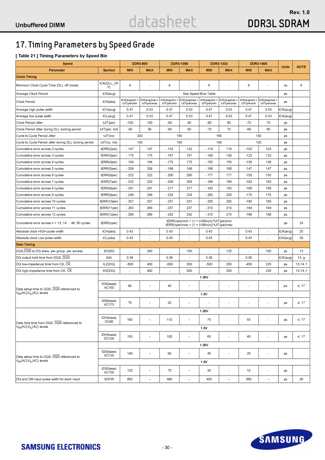
17. Timing Parameters by Speed Grade
[ Table 21 ] Timing Parameters by Speed Bin
|
|
|
|
|
|
| Speed |
| Units | NOTE | |||||||||||||||
|
| Parameter | Symbol | MIN |
| MAX | MIN | MAX | MIN | MAX | MIN |
| MAX | ||||||||||||
|
|
|
|
|
| ||||||||||||||||||||
Clock Timing |
|
|
|
|
|
|
|
|
|
|
|
|
| ||||||||||||
Minimum Clock Cycle Time (DLL off mode) | tCK(DLL_OF | 8 |
| - | 8 | - | 8 | - | 8 |
| - | ns | 6 | ||||||||||||
F) |
|
| |||||||||||||||||||||||
|
|
|
|
|
|
|
|
|
|
|
|
|
|
|
|
|
|
|
|
|
|
|
|
| |
|
|
|
|
|
|
|
|
|
|
|
|
|
| ||||||||||||
Average Clock Period | tCK(avg) |
|
|
|
| See Speed Bins Table |
|
|
|
| ps |
| |||||||||||||
|
|
|
|
|
|
|
|
|
|
|
|
|
|
|
|
|
|
|
|
|
|
|
| ||
Clock Period | tCK(abs) | tCK(avg)min + | tCK(avg)max + | tCK(avg)min + | tCK(avg)max + | tCK(avg)min + | tCK(avg)max + | tCK(avg)min + | tCK(avg)max + | ps |
| ||||||||||||||
tJIT(per)min | tJIT(per)max | tJIT(per)min | tJIT(per)max | tJIT(per)min | tJIT(per)max | tJIT(per)min | tJIT(per)max |
| |||||||||||||||||
|
|
|
|
|
|
|
|
|
|
|
|
|
|
|
| ||||||||||
|
|
|
|
|
|
|
|
|
|
|
|
|
| ||||||||||||
Average high pulse width | tCH(avg) | 0.47 |
| 0.53 | 0.47 | 0.53 | 0.47 | 0.53 | 0.47 |
| 0.53 | tCK(avg) |
| ||||||||||||
|
|
|
|
|
|
|
|
|
|
|
|
|
| ||||||||||||
Average low pulse width | tCL(avg) | 0.47 |
| 0.53 | 0.47 | 0.53 | 0.47 | 0.53 | 0.47 |
| 0.53 | tCK(avg) |
| ||||||||||||
|
|
|
|
|
|
|
|
|
|
|
|
|
| ||||||||||||
Clock Period Jitter | tJIT(per) |
| 100 | 90 | 80 |
| 70 | ps |
| ||||||||||||||||
|
|
|
|
|
|
|
|
|
|
|
|
|
| ||||||||||||
Clock Period Jitter during DLL locking period | tJIT(per, lck) |
| 90 | 80 | 70 |
| 60 | ps |
| ||||||||||||||||
|
|
|
|
|
|
|
|
|
|
|
|
|
| ||||||||||||
Cycle to Cycle Period Jitter | tJIT(cc) |
| 200 | 180 | 160 | 140 |
| ps |
| ||||||||||||||||
|
|
|
|
|
|
|
|
|
| ||||||||||||||||
Cycle to Cycle Period Jitter during DLL locking period | tJIT(cc, lck) |
| 180 | 160 | 140 | 120 |
| ps |
| ||||||||||||||||
|
|
|
|
|
|
|
|
|
|
|
|
|
| ||||||||||||
Cumulative error across 2 cycles | tERR(2per) | - 147 |
| 147 | - 132 | 132 | - 118 | 118 |
| 103 | ps |
| |||||||||||||
|
|
|
|
|
|
|
|
|
|
|
|
|
| ||||||||||||
Cumulative error across 3 cycles | tERR(3per) | - 175 |
| 175 | - 157 | 157 | - 140 | 140 |
| 122 | ps |
| |||||||||||||
|
|
|
|
|
|
|
|
|
|
|
|
|
| ||||||||||||
Cumulative error across 4 cycles | tERR(4per) | - 194 |
| 194 | - 175 | 175 | - 155 | 155 |
| 136 | ps |
| |||||||||||||
|
|
|
|
|
|
|
|
|
|
|
|
|
| ||||||||||||
Cumulative error across 5 cycles | tERR(5per) | - 209 |
| 209 | - 188 | 188 | - 168 | 168 |
| 147 | ps |
| |||||||||||||
|
|
|
|
|
|
|
|
|
|
|
|
|
| ||||||||||||
Cumulative error across 6 cycles | tERR(6per) | - 222 |
| 222 | - 200 | 200 | - 177 | 177 |
| 155 | ps |
| |||||||||||||
|
|
|
|
|
|
|
|
|
|
|
|
|
| ||||||||||||
Cumulative error across 7 cycles | tERR(7per) | - 232 |
| 232 | - 209 | 209 | - 186 | 186 |
| 163 | ps |
| |||||||||||||
|
|
|
|
|
|
|
|
|
|
|
|
|
| ||||||||||||
Cumulative error across 8 cycles | tERR(8per) | - 241 |
| 241 | - 217 | 217 | - 193 | 193 |
| 169 | ps |
| |||||||||||||
|
|
|
|
|
|
|
|
|
|
|
|
|
| ||||||||||||
Cumulative error across 9 cycles | tERR(9per) | - 249 |
| 249 | - 224 | 224 | - 200 | 200 |
| 175 | ps |
| |||||||||||||
|
|
|
|
|
|
|
|
|
|
|
|
|
| ||||||||||||
Cumulative error across 10 cycles | tERR(10per) | - 257 |
| 257 | - 231 | 231 | - 205 | 205 |
| 180 | ps |
| |||||||||||||
|
|
|
|
|
|
|
|
|
|
|
|
|
| ||||||||||||
Cumulative error across 11 cycles | tERR(11per) | - 263 |
| 263 | - 237 | 237 | - 210 | 210 |
| 184 | ps |
| |||||||||||||
|
|
|
|
|
|
|
|
|
|
|
|
|
| ||||||||||||
Cumulative error across 12 cycles | tERR(12per) | - 269 |
| 269 | - 242 | 242 | - 215 | 215 |
| 188 | ps |
| |||||||||||||
|
|
|
|
|
|
|
|
|
|
|
|
|
|
|
|
|
|
|
|
|
|
|
|
|
|
Cumulative error across n = 13, 14 ... 49, 50 cycles | tERR(nper) |
|
|
| tERR(nper)min = (1 + 0.68ln(n))*tJIT(per)min |
|
|
| ps | 24 | |||||||||||||||
|
|
| tERR(nper)max = (1 = 0.68ln(n))*tJIT(per)max |
|
|
| |||||||||||||||||||
|
|
|
|
|
|
|
|
|
|
|
|
|
|
|
|
|
|
|
|
|
| ||||
|
|
|
|
|
|
|
|
|
|
|
|
|
| ||||||||||||
Absolute clock HIGH pulse width | tCH(abs) | 0.43 |
| - | 0.43 | - | 0.43 | - | 0.43 |
| - | tCK(avg) | 25 | ||||||||||||
|
|
|
|
|
|
|
|
|
|
|
|
|
| ||||||||||||
Absolute clock Low pulse width | tCL(abs) | 0.43 |
| - | 0.43 | - | 0.43 | - | 0.43 |
| - | tCK(avg) | 26 | ||||||||||||
|
|
|
|
|
|
|
|
|
|
|
|
|
|
|
|
|
|
|
|
|
|
|
|
|
|
Data Timing |
|
|
|
|
|
|
|
|
|
|
|
|
| ||||||||||||
|
| to DQ skew, per group, per access | tDQSQ | - |
| 200 | - | 150 | - | 125 | - |
| 100 | ps | 13 | ||||||||||
DQS,DQS |
|
| |||||||||||||||||||||||
|
|
|
|
|
|
|
|
|
|
|
|
|
|
|
|
|
|
|
| ||||||
DQ output hold time from DQS, |
|
|
|
|
|
| tQH | 0.38 |
| - | 0.38 | - | 0.38 | - | 0.38 |
| - | tCK(avg) | 13, g | ||||||
DQS |
|
| |||||||||||||||||||||||
|
|
|
|
|
|
|
|
|
|
|
|
|
|
|
|
|
| ||||||||
DQ |
|
|
|
|
| tLZ(DQ) |
| 400 | 300 | 250 |
| 225 | ps | 13,14, f | |||||||||||
CK |
|
| |||||||||||||||||||||||
|
|
|
|
|
|
|
|
|
|
|
|
|
|
|
| ||||||||||
DQ |
|
|
|
| tHZ(DQ) | - |
| 400 | - | 300 | - | 250 | - |
| 225 | ps | 13,14, f | ||||||||
CK |
|
| |||||||||||||||||||||||
|
|
|
|
|
|
|
|
|
|
|
|
|
|
|
|
|
|
|
|
|
|
|
|
|
|
|
|
|
|
|
|
|
|
|
|
|
|
|
|
|
|
|
|
| 1.35V |
|
|
|
|
|
|
|
|
|
|
|
|
|
|
|
|
|
|
|
|
|
|
|
|
|
|
|
|
|
|
|
|
|
|
|
|
|
|
|
|
|
|
|
|
| tDS(base) | 90 |
| - | 40 | - | - | - | - |
| - | ps | d, 17 |
|
|
|
|
|
|
|
|
|
|
|
|
| AC160 |
|
| ||||||||||
Data setup time to DQS, DQS referenced to |
|
|
|
|
|
|
|
|
|
|
|
| |||||||||||||
|
|
|
|
|
|
|
|
|
|
|
|
| |||||||||||||
VIH(AC)VIL(AC) levels |
|
|
|
|
|
| 1.5V |
|
|
|
|
|
| ||||||||||||
|
|
|
|
|
|
|
|
|
|
|
|
| tDS(base) | 75 |
| - | 25 | - | - | - | - |
| - | ps | d, 17 |
|
|
|
|
|
|
|
|
|
|
|
|
| AC175 |
|
| ||||||||||
|
|
|
|
|
|
|
|
|
|
|
|
|
|
|
|
|
|
|
|
|
|
|
|
| |
|
|
|
|
|
|
|
|
|
|
|
|
|
|
|
|
|
|
|
|
|
|
|
|
|
|
|
|
|
|
|
|
|
|
|
|
|
|
|
|
|
|
|
|
| 1.35V |
|
|
|
|
|
|
|
|
|
|
|
|
|
|
|
|
|
|
|
|
|
|
|
|
|
|
|
|
|
|
|
|
|
|
|
|
|
|
|
|
|
|
|
|
| tDH(base) | 160 |
| - | 110 | - | 75 | - | 55 |
| - | ps | d, 17 |
|
|
|
|
|
|
|
|
|
|
|
|
| DC90 |
|
| ||||||||||
Data hold time from DQS, DQS referenced to |
|
|
|
|
|
|
|
|
|
|
|
| |||||||||||||
|
|
|
|
|
|
|
|
|
|
|
|
| |||||||||||||
VIH(AC)VIL(AC) levels |
|
|
|
|
|
| 1.5V |
|
|
|
|
|
| ||||||||||||
|
|
|
|
|
|
|
|
|
|
|
|
| tDH(base) | 150 |
| - | 100 | - | 65 | - | 45 |
| - | ps | d, 17 |
|
|
|
|
|
|
|
|
|
|
|
|
| DC100 |
|
| ||||||||||
|
|
|
|
|
|
|
|
|
|
|
|
|
|
|
|
|
|
|
|
|
|
|
|
| |
|
|
|
|
|
|
|
|
|
|
|
|
|
|
|
|
|
|
|
|
|
|
|
|
|
|
|
|
|
|
|
|
|
|
|
|
|
|
|
|
|
|
|
|
| 1.35V |
|
|
|
|
|
|
|
|
|
|
|
|
|
|
|
|
|
|
|
|
|
|
|
|
|
|
|
|
|
|
|
|
|
|
|
|
|
|
|
|
|
|
|
|
| tDS(base) | 140 |
| - | 90 | - | 45 | - | 25 |
| - | ps |
|
|
|
|
|
|
|
|
|
|
|
|
|
| AC135 |
|
|
| |||||||||
Data setup time to DQS, DQS referenced to |
|
|
|
|
|
|
|
|
|
|
|
| |||||||||||||
|
|
|
|
|
|
|
|
|
|
|
|
| |||||||||||||
VIH(AC)VIL(AC) levels |
|
|
|
|
|
| 1.5V |
|
|
|
|
|
| ||||||||||||
|
|
|
|
|
|
|
|
|
|
|
|
| tDS(base) | 125 |
| - | 75 | - | 30 | - | 10 |
| - | ps |
|
|
|
|
|
|
|
|
|
|
|
|
|
| AC150 |
|
|
| |||||||||
|
|
|
|
|
|
|
|
|
|
|
|
|
|
|
|
|
|
|
|
|
|
|
|
| |
|
|
|
|
|
|
|
|
|
|
|
|
|
| ||||||||||||
DQ and DM Input pulse width for each input | tDIPW | 600 |
| - | 490 | - | 400 | - | 360 |
| - | ps | 28 | ||||||||||||
|
|
|
|
|
|
|
|
|
|
|
|
|
|
|
|
|
|
|
|
|
|
|
|
|
|
- 30 -