Samsung M391B5273DH0 Vref Tolerances, Illustration of Vrefdc tolerance and Vref ac-noise limits

Models: M391B5773DH0 M391B5273DH0

1 36
Download 36 pages 22.54 Kb
Page 14
Image 14

Unbuffered DIMM

datasheet

Rev. 1.0

DDR3L SDRAM

11.2 VREF Tolerances
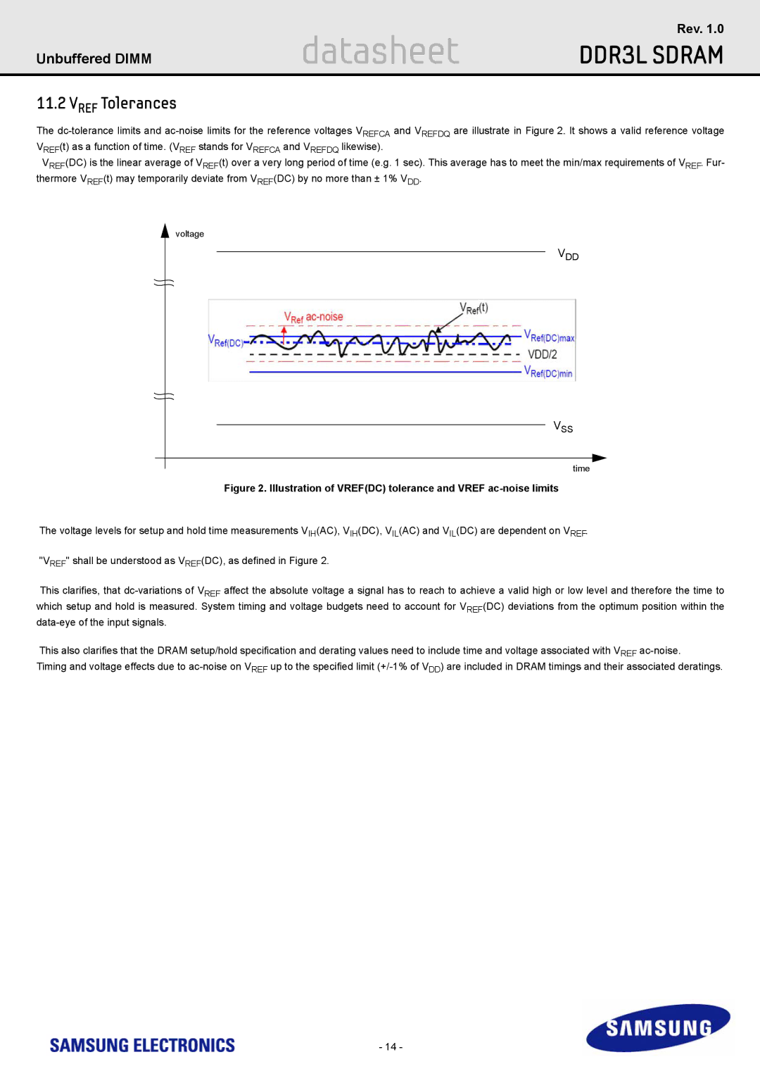
The dc-tolerance limits and ac-noise limits for the reference voltages VREFCA and VREFDQ are illustrate in Figure 2. It shows a valid reference voltage VREF(t) as a function of time. (VREF stands for VREFCA and VREFDQ likewise).

VREF(DC) is the linear average of VREF(t) over a very long period of time (e.g. 1 sec). This average has to meet the min/max requirements of VREF. Fur- thermore VREF(t) may temporarily deviate from VREF(DC) by no more than ± 1% VDD.

voltage

VDD

VSS

time

Figure 2. Illustration of VREF(DC) tolerance and VREF ac-noise limits

The voltage levels for setup and hold time measurements VIH(AC), VIH(DC), VIL(AC) and VIL(DC) are dependent on VREF.

"VREF" shall be understood as VREF(DC), as defined in Figure 2.

This clarifies, that dc-variations of VREF affect the absolute voltage a signal has to reach to achieve a valid high or low level and therefore the time to which setup and hold is measured. System timing and voltage budgets need to account for VREF(DC) deviations from the optimum position within the data-eye of the input signals.

This also clarifies that the DRAM setup/hold specification and derating values need to include time and voltage associated with VREF ac-noise.

Timing and voltage effects due to ac-noise on VREF up to the specified limit (+/-1% of VDD) are included in DRAM timings and their associated deratings.

- 14 -

Page 14
Image 14
Samsung M391B5273DH0, M391B5773DH0 specifications Vref Tolerances, Illustration of Vrefdc tolerance and Vref ac-noise limits