Unbuffered DIMM
datasheet
Rev. 1.0
DDR3L SDRAM
5. Pin Description
| Pin Name | Description |
| Pin Name | Description | |||||||||||
| SDRAM address bus | SCL | I2C serial bus clock for EEPROM | |||||||||||||
| SDRAM bank select | SDA | I2C serial bus data line for EEPROM | |||||||||||||
|
|
|
|
|
|
|
|
|
|
|
| SDRAM row address strobe | I2C serial address select for EEPROM | |||
| RAS | |||||||||||||||
|
|
|
|
|
|
|
|
|
|
|
| SDRAM column address strobe |
| VDD* | SDRAM core power supply | |
| CAS | |||||||||||||||
|
|
|
|
|
|
|
|
|
|
| SDRAM write enable |
| VDDQ* | SDRAM I/O Driver power supply | ||
| WE | |||||||||||||||
|
|
|
|
|
|
|
|
|
|
|
| DIMM Rank Select Lines |
| VREFDQ | SDRAM I/O reference supply | |
| S0, S1 | |||||||||||||||
| CKE0,CKE1 | SDRAM clock enable lines |
| VREFCA | SDRAM command/address reference supply | |||||||||||
| ODT0, ODT1 |
| VSS | Power supply return (ground) | ||||||||||||
| DQ0 - DQ63 | DIMM memory data bus |
| VDDSPD | Serial EEPROM positive power supply | |||||||||||
| CB0 - CB7 | DIMM ECC check bits | NC | Spare Pins(no connect) | ||||||||||||
|
|
|
|
|
|
|
|
|
|
|
|
|
|
|
|
|
| DQS0 - DQS8 | SDRAM data strobes |
| TEST | Used by memory bus analysis tools | |||||||||||
| (positive line of differential pair) |
| (unused on memory DIMMs) | |||||||||||||
|
|
|
|
|
|
|
|
|
|
|
|
|
|
| ||
|
|
|
|
|
|
|
|
|
|
|
|
|
|
|
|
|
|
|
|
|
|
|
|
|
|
|
|
| SDRAM differential data strobes |
|
|
|
|
|
| RESET | Set DRAMs Known State | |||||||||||||
| (negative line of differential pair) |
| ||||||||||||||
|
|
|
|
|
|
|
|
|
|
|
|
|
|
|
| |
|
|
|
|
|
|
|
|
|
|
|
|
|
|
|
|
|
| SDRAM data masks/high data strobes |
|
|
| Reserved for optional | |||||||||||
|
| EVENT | ||||||||||||||
|
| |||||||||||||||
|
|
|
|
|
|
|
|
|
|
|
|
|
|
|
| |
|
|
|
|
|
|
|
|
|
|
|
|
|
|
|
|
|
| CK0, CK1 | SDRAM clocks |
| VTT | SDRAM I/O termination supply | |||||||||||
| (positive line of differential pair) |
| ||||||||||||||
|
|
|
|
|
|
|
|
|
|
|
|
|
|
|
| |
|
|
|
|
|
|
|
|
|
|
|
|
|
|
|
|
|
|
|
|
|
|
|
|
|
|
|
|
| SDRAM clocks |
|
|
|
|
| CK0, CK1 |
| RFU | Reserved for future use | ||||||||||||
| (negative line of differential pair) |
| ||||||||||||||
|
|
|
|
|
|
|
|
|
|
|
|
|
|
|
| |
|
|
|
|
|
|
|
|
|
|
|
|
|
|
|
|
|
NOTE :
*The VDD and VDDQ pins are tied common to a single
**DM8, DQS8 and DQS8 are for ECC UDIMM only.
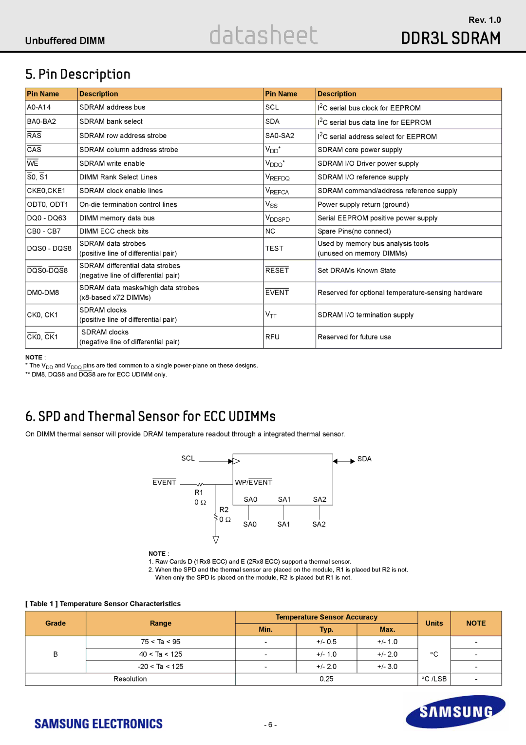
6. SPD and Thermal Sensor for ECC UDIMMs
On DIMM thermal sensor will provide DRAM temperature readout through a integrated thermal sensor.
|
| SCL |
|
|
|
|
|
|
|
|
|
|
| SDA | ||
|
|
|
|
|
|
|
|
|
|
|
|
|
|
|
|
|
EVENT |
|
|
|
|
| WP/EVENT |
|
|
|
|
|
|
| |||
R1 |
|
|
|
|
|
|
|
|
| |||||||
|
|
|
| SA0 | SA1 | SA2 |
|
|
| |||||||
|
| 0 Ω |
|
|
|
|
| |||||||||
|
|
|
|
| R2 |
|
|
|
|
|
|
|
|
|
| |
|
|
|
|
| 0 Ω |
|
|
|
|
|
|
|
|
|
| |
|
|
|
|
| SA0 | SA1 | SA2 | |||||||||
|
|
|
|
| ||||||||||||
|
|
|
|
|
|
| ||||||||||
|
|
|
|
|
|
|
|
|
|
|
|
|
|
|
|
|
NOTE :
1.Raw Cards D (1Rx8 ECC) and E (2Rx8 ECC) support a thermal sensor.
2.When the SPD and the thermal sensor are placed on the module, R1 is placed but R2 is not. When only the SPD is placed on the module, R2 is placed but R1 is not.
[ Table 1 ] Temperature Sensor Characteristics
Grade | Range | Temperature Sensor Accuracy | Units | NOTE | |||
Min. | Typ. | Max. | |||||
|
|
|
| ||||
| 75 < Ta < 95 | - | +/- 0.5 | +/- 1.0 |
| - | |
|
|
|
|
|
|
| |
B | 40 < Ta < 125 | - | +/- 1.0 | +/- 2.0 | °C | - | |
|
|
|
|
|
|
| |
| - | +/- 2.0 | +/- 3.0 |
| - | ||
|
|
|
|
|
|
| |
| Resolution |
| 0.25 |
| °C /LSB | - | |
|
|
|
|
|
|
| |
|
| - 6 - |
|
|
|
| |