Unbuffered DIMM
datasheet
Rev. 1.0
DDR3L SDRAM
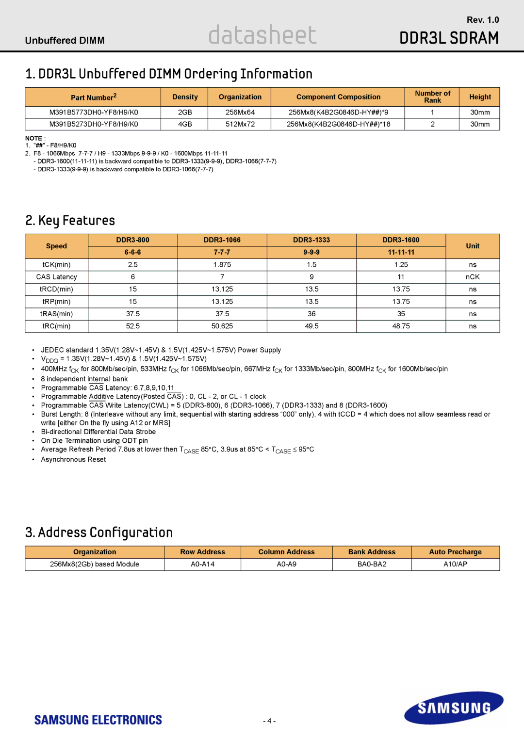
1. DDR3L Unbuffered DIMM Ordering Information
Part Number2 | Density | Organization | Component Composition | Number of | Height | |
Rank | ||||||
|
|
|
|
| ||
2GB | 256Mx64 | 1 | 30mm | |||
|
|
|
|
|
| |
4GB | 512Mx72 | 2 | 30mm | |||
|
|
|
|
|
|
NOTE :
1."##" - F8/H9/K0
2.F8 - 1066Mbps
-
-
2. Key Features
Speed |
|
|
|
| Unit | |
|
| |||||
tCK(min) | 2.5 | 1.875 | 1.5 | 1.25 | ns | |
|
|
|
|
|
| |
CAS Latency | 6 | 7 | 9 | 11 | nCK | |
|
|
|
|
|
| |
tRCD(min) | 15 | 13.125 | 13.5 | 13.75 | ns | |
|
|
|
|
|
| |
tRP(min) | 15 | 13.125 | 13.5 | 13.75 | ns | |
|
|
|
|
|
| |
tRAS(min) | 37.5 | 37.5 | 36 | 35 | ns | |
|
|
|
|
|
| |
tRC(min) | 52.5 | 50.625 | 49.5 | 48.75 | ns | |
|
|
|
|
|
|
•JEDEC standard 1.35V(1.28V~1.45V) & 1.5V(1.425V~1.575V) Power Supply
•VDDQ = 1.35V(1.28V~1.45V) & 1.5V(1.425V~1.575V)
•400MHz fCK for 800Mb/sec/pin, 533MHz fCK for 1066Mb/sec/pin, 667MHz fCK for 1333Mb/sec/pin, 800MHz fCK for 1600Mb/sec/pin
•8 independent internal bank
•Programmable CAS Latency: 6,7,8,9,10,11
•Programmable Additive Latency(Posted CAS) : 0, CL - 2, or CL - 1 clock
•Programmable CAS Write Latency(CWL) = 5
•Burst Length: 8 (Interleave without any limit, sequential with starting address “000” only), 4 with tCCD = 4 which does not allow seamless read or write [either On the fly using A12 or MRS]
•
•On Die Termination using ODT pin
•Average Refresh Period 7.8us at lower then TCASE 85°C, 3.9us at 85°C < TCASE ≤ 95°C
•Asynchronous Reset
3. Address Configuration
Organization | Row Address | Column Address | Bank Address | Auto Precharge |
256Mx8(2Gb) based Module | A10/AP | |||
|
|
|
|
|
- 4 -
