CAPACITANCE (TA = 25°C; fC = 1MHz; VDD = 0V)
Output and I/O pins capacitive load specified as follows:
PARAMETER | SYMBOL | MIN | TYP | MAX | UNIT | COMMENT |
|
|
|
|
|
|
|
Input Capacitance | CIN |
|
| 5.0 | pF |
|
|
|
|
|
|
|
|
Output Capacitance 1 | COUT1 |
|
| 45 | pF | Maximum |
(All outputs except |
|
|
|
|
| Capacitive Load |
nPULSE1 in BackPlane |
|
|
|
|
| which can be |
Mode) |
|
|
|
|
| supported by each |
Output Capacitance 2 | COUT2 |
|
| 400 | pF | output. |
(nPULSE1, in |
|
|
|
|
|
|
BackPlane |
|
|
|
|
|
|
Mode Only - Open |
|
|
|
|
|
|
Drain) |
|
|
|
|
|
|
|
|
|
|
|
|
|
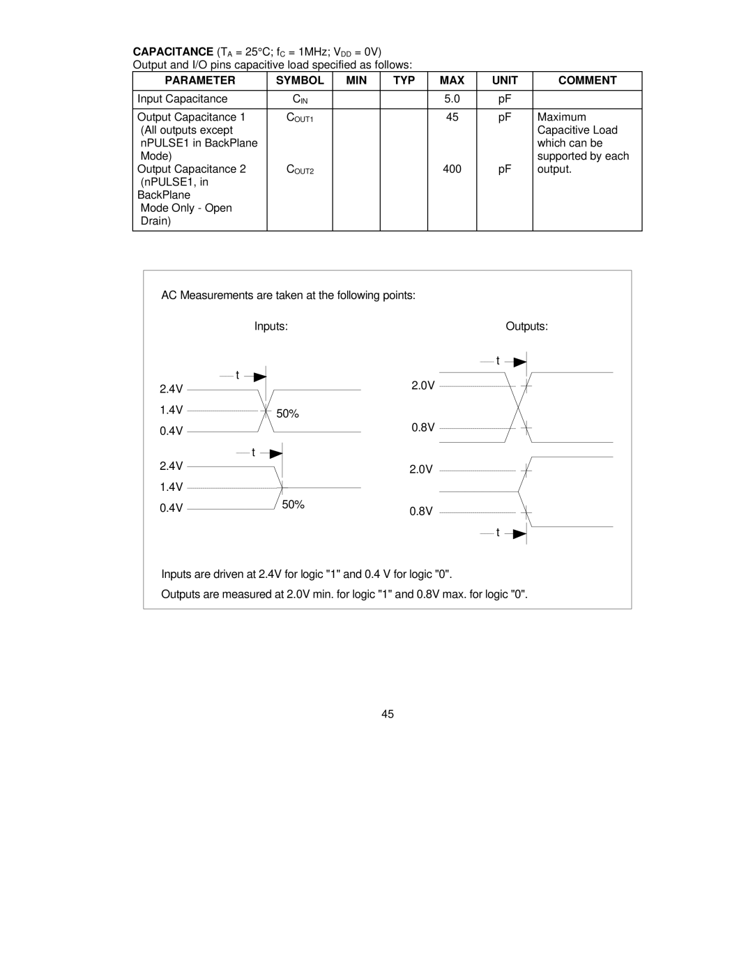
AC Measurements are taken at the following points:
Inputs:Outputs:
t
| t |
2.4V | 2.0V |
| |
1.4V | 50% |
|
0.4V | 0.8V |
|
2.4V | t |
|
| ||
|
| 2.0V | |||
|
|
|
| ||
1.4V |
|
|
|
|
|
|
|
|
|
| |
|
|
|
|
| |
0.4V | 50% | ||||
|
|
|
| 0.8V | |
t
Inputs are driven at 2.4V for logic "1" and 0.4 V for logic "0".
Outputs are measured at 2.0V min. for logic "1" and 0.8V max. for logic "0".
45