Contents
Features
General Description
Table of Contents
PIN Configuration
Description of PIN Functions
A1,A2/ALE
Miscellaneous
DIP PIN Plcc PIN Name Symbol Description
Transmission Media Interface
Instead, it must be connected to XTAL1 with
COM20020 Operation
Network Reconfiguration
Protocol Description
Network Protocol
Data Rates
Response Time
Extended Timeout Function
Broadcast Messages
Reconfiguration Time
Idle Time
Line Protocol
Invitations To Transmit
Negative Acknowledgements
Data Packets
Acknowledgements
System Description
MULTIPLEXED, 8051-LIKE BUS Interface with RS-485 Interface
Figure C
Backplane Configuration
Traditional Hybrid Interface
COM20020 Network Using RS-485 Differential Transceivers
Differential Driver Configuration
Programmable Txen Polarity
Internal Block Diagram
Functional Description
Attenuation
Nominal
Cable Type Impedance AT 5MHZ
Read Register Summary
Write
Internal Registers
Interrupt Mask Register IMR
Data Register
Tentative ID Register
Diagnostic Status Register
Command Register
Next ID Register
Status Register
Configuration Register Setup Register
BIT BIT Name Symbol Description
BIT BIT Name Symbol Description
Dupid
Data Command Description
Address Pointer High Register
Address Pointer Low Register
Configuration Register
Reset
CKP3 CKP2 CKP1
Sequential Access Operation
Sequential Access Memory
Access Speed
Internal RAM
Software Interface
Selecting RAM Page Size
Transmit Sequence
RAM Buffer Packet Configuration
Page
Receive Sequence
Command Chaining
Transmit Command Chaining
Receive Command Chaining
Reset Details
Internal Reset Logic
Improved Diagnostics
Initialization Sequence
Normal Results
Abnormal Results
Oscillator
Maximum Guaranteed Ratings
DC Electrical Characteristics
Parameter Symbol MIN TYP MAX Unit Comment
Operational Description
XTAL1, XTAL2
Input Capacitance
Timing Diagrams
Multiplexed BUS, 68XX-LIKE Control Signals Read Cycle
Multiplexed BUS, 80XX-LIKE Control Signals Read Cycle
Multiplexed BUS, 68XX-LIKE Control Signals Write Cycle
Multiplexed BUS, 80XX-LIKE Control Signals Write Cycle
NON-MULTIPLEXED BUS, 80XX-LIKE Control Signals Read Cycle
NON-MULTIPLEXED BUS, 68XX-LIKE Control Signals Read Cycle
NON-MULTIPLEXED BUS, 80XX-LIKE Control Signals Write Cycle
NON-MULTIPLEXED BUS, 68XX-LIKE Control Signals Write Cycle
Normal Mode Transmit or Receive Timing
These signals are to and from the hybrid
NTXEN NPULSE1
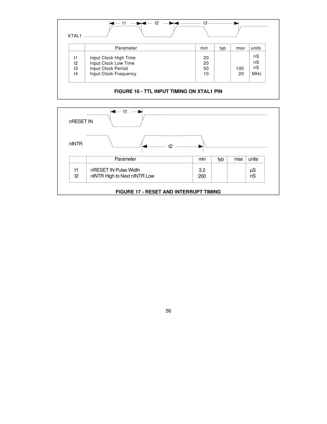
TTL Input Timing on XTAL1 PIN
28-PIN Plcc Package Dimensions
24-PIN DIP Package Dimensions
Date
SECTION/FIGURE/ENTRY Correction Revised
Standard Microsystems Corp