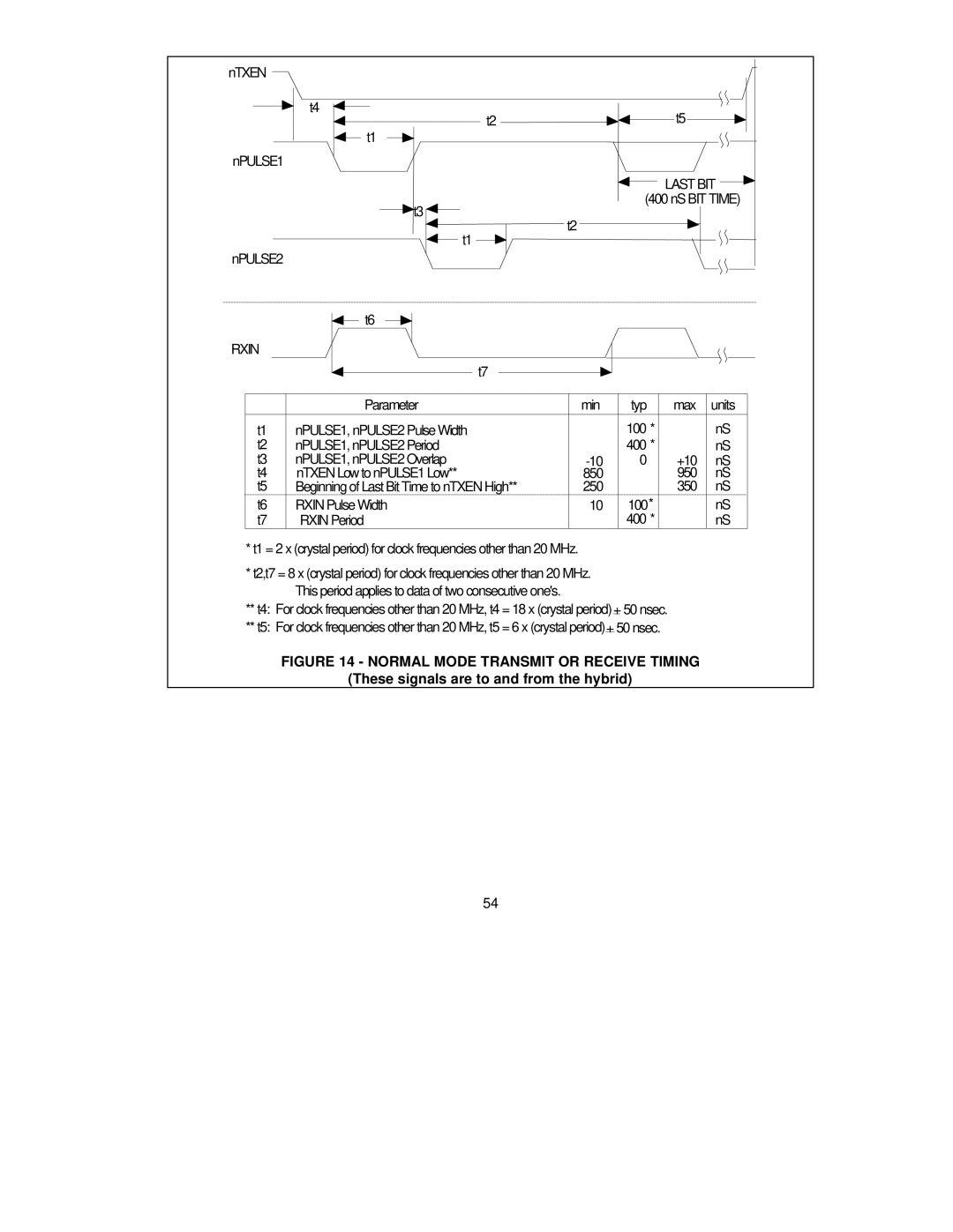
nTXEN
t4
nPULSE1
nPULSE2
t2 | t5 | |
t1 |
| |
| LAST BIT | |
t3 | (400 nS BIT TIME) | |
t2 | ||
t1 | ||
|
RXIN
t6
t7
| Parameter | min | typ |
| max | units |
t1 | nPULSE1, nPULSE2 Pulse Width |
| 100 | * |
| nS |
t2 | nPULSE1, nPULSE2 Period |
| 400 | * |
| nS |
t3 | nPULSE1, nPULSE2 Overlap | 0 |
| +10 | nS | |
t4 | nTXEN Low to nPULSE1 Low** | 850 |
|
| 950 | nS |
t5 | Beginning of Last Bit Time to nTXEN High** | 250 |
|
| 350 | nS |
t6 | RXIN Pulse Width | 10 | 100* |
| nS | |
t7 | RXIN Period |
| 400 | * |
| nS |
*t1 = 2 x (crystal period) for clock frequencies other than 20 MHz.
*t2,t7 = 8 x (crystal period) for clock frequencies other than 20 MHz. This period applies to data of two consecutive one's.
**t4: For clock frequencies other than 20 MHz, t4 = 18 x (crystal period)+ 50 nsec.
**t5: For clock frequencies other than 20 MHz, t5 = 6 x (crystal period)+ 50 nsec.
FIGURE 14 - NORMAL MODE TRANSMIT OR RECEIVE TIMING
(These signals are to and from the hybrid)
54