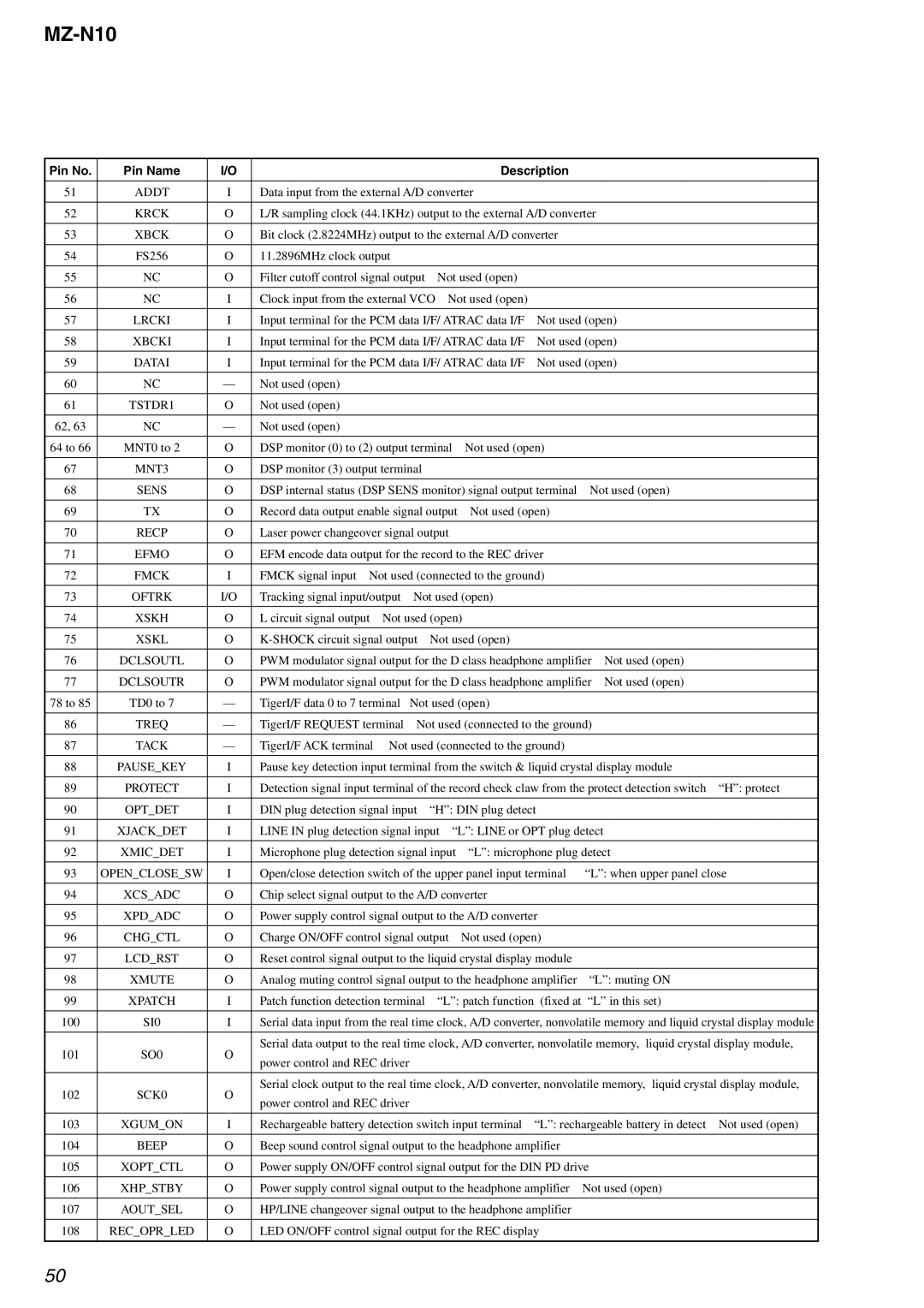
MZ-N10
Pin No. | Pin Name | I/O |
|
|
|
|
| Description |
|
|
|
| |
|
|
|
|
|
|
|
|
| |||||
51 | ADDT | I | Data input from the external A/D converter |
|
|
|
|
| |||||
|
|
|
|
|
|
| |||||||
52 | KRCK | O | L/R sampling clock (44.1KHz) output to the external A/D converter |
|
|
| |||||||
|
|
|
|
|
|
|
| ||||||
53 | XBCK | O | Bit clock (2.8224MHz) output to the external A/D converter |
|
|
|
| ||||||
|
|
|
|
|
|
|
|
|
|
|
|
| |
54 | FS256 | O | 11.2896MHz clock output |
|
|
|
|
|
|
|
|
| |
|
|
|
|
|
|
|
|
|
| ||||
55 | NC | O | Filter cutoff control signal output | Not used (open) |
|
|
|
|
| ||||
|
|
|
|
|
|
|
|
|
| ||||
56 | NC | I | Clock input from the external VCO | Not used (open) |
|
|
|
|
| ||||
|
|
|
|
|
|
| |||||||
57 | LRCKI | I | Input terminal for the PCM data I/F/ ATRAC data I/F | Not used (open) |
|
| |||||||
|
|
|
|
|
|
| |||||||
58 | XBCKI | I | Input terminal for the PCM data I/F/ ATRAC data I/F | Not used (open) |
|
| |||||||
|
|
|
|
|
|
| |||||||
59 | DATAI | I | Input terminal for the PCM data I/F/ ATRAC data I/F | Not used (open) |
|
| |||||||
|
|
|
|
|
|
|
|
|
|
|
|
|
|
60 | NC | — | Not used (open) |
|
|
|
|
|
|
|
|
|
|
|
|
|
|
|
|
|
|
|
|
|
|
|
|
61 | TSTDR1 | O | Not used (open) |
|
|
|
|
|
|
|
|
|
|
|
|
|
|
|
|
|
|
|
|
|
|
|
|
62, 63 | NC | — | Not used (open) |
|
|
|
|
|
|
|
|
|
|
|
|
|
|
|
|
|
|
| |||||
64 to 66 | MNT0 to 2 | O | DSP monitor (0) to (2) output terminal | Not used (open) |
|
|
|
| |||||
|
|
|
|
|
|
|
|
|
|
|
| ||
67 | MNT3 | O | DSP monitor (3) output terminal |
|
|
|
|
|
|
|
| ||
|
|
|
|
|
| ||||||||
68 | SENS | O | DSP internal status (DSP SENS monitor) signal output terminal | Not used (open) |
| ||||||||
|
|
|
|
|
|
|
|
| |||||
69 | TX | O | Record data output enable signal output | Not used (open) |
|
|
|
| |||||
|
|
|
|
|
|
|
|
|
| ||||
70 | RECP | O | Laser power changeover signal output |
|
|
|
|
|
| ||||
|
|
|
|
|
|
|
| ||||||
71 | EFMO | O | EFM encode data output for the record to the REC driver |
|
|
|
| ||||||
|
|
|
|
|
|
|
| ||||||
72 | FMCK | I | FMCK signal input Not used (connected to the ground) |
|
|
|
| ||||||
|
|
|
|
|
|
|
|
|
| ||||
73 | OFTRK | I/O | Tracking signal input/output | Not used (open) |
|
|
|
|
| ||||
|
|
|
|
|
|
|
|
|
| ||||
74 | XSKH | O | L circuit signal output | Not used (open) |
|
|
|
|
| ||||
|
|
|
|
|
|
|
|
|
| ||||
75 | XSKL | O | Not used (open) |
|
|
|
|
| |||||
|
|
|
|
|
| ||||||||
76 | DCLSOUTL | O | PWM modulator signal output for the D class headphone amplifier | Not used (open) |
| ||||||||
|
|
|
|
|
| ||||||||
77 | DCLSOUTR | O | PWM modulator signal output for the D class headphone amplifier | Not used (open) |
| ||||||||
|
|
|
|
|
|
|
|
|
| ||||
78 to 85 | TD0 to 7 | — | TigerI/F data 0 to 7 terminal | Not used (open) |
|
|
|
|
| ||||
|
|
|
|
|
|
|
| ||||||
86 | TREQ | — | TigerI/F REQUEST terminal | Not used (connected to the ground) |
|
|
| ||||||
|
|
|
|
|
|
|
|
| |||||
87 | TACK | — | TigerI/F ACK terminal | Not used (connected to the ground) |
|
|
|
| |||||
|
|
|
|
| |||||||||
88 | PAUSE_KEY | I | Pause key detection input terminal from the switch & liquid crystal display module |
| |||||||||
|
|
|
|
| |||||||||
89 | PROTECT | I | Detection signal input terminal of the record check claw from the protect detection switch | “H”: protect | |||||||||
|
|
|
|
|
|
|
|
| |||||
90 | OPT_DET | I | DIN plug detection signal input | “H”: DIN plug detect |
|
|
|
| |||||
|
|
|
|
|
|
|
| ||||||
91 | XJACK_DET | I | LINE IN plug detection signal input | “L”: LINE or OPT plug detect |
|
|
| ||||||
|
|
|
|
|
|
| |||||||
92 | XMIC_DET | I | Microphone plug detection signal input | “L”: microphone plug detect |
|
| |||||||
|
|
|
|
| |||||||||
93 | OPEN_CLOSE_SW | I | Open/close detection switch of the upper panel input terminal | “L”: when upper panel close | |||||||||
|
|
|
|
|
|
|
|
| |||||
94 | XCS_ADC | O | Chip select signal output to the A/D converter |
|
|
|
|
| |||||
|
|
|
|
|
|
|
| ||||||
95 | XPD_ADC | O | Power supply control signal output to the A/D converter |
|
|
|
| ||||||
|
|
|
|
|
|
|
|
| |||||
96 | CHG_CTL | O | Charge ON/OFF control signal output | Not used (open) |
|
|
|
| |||||
|
|
|
|
|
|
|
| ||||||
97 | LCD_RST | O | Reset control signal output to the liquid crystal display module |
|
|
|
| ||||||
|
|
|
|
|
| ||||||||
98 | XMUTE | O | Analog muting control signal output to the headphone amplifier | “L”: muting ON |
| ||||||||
|
|
|
|
|
|
|
| ||||||
99 | XPATCH | I | Patch function detection terminal | “L”: patch function | (fixed at | “L” in this set) |
| ||||||
|
|
|
| ||||||||||
100 | SI0 | I | Serial data input from the real time clock, A/D converter, nonvolatile memory and liquid crystal display module | ||||||||||
|
|
|
|
| |||||||||
101 | SO0 | O | Serial data output to the real time clock, A/D converter, nonvolatile memory, | liquid crystal display module, | |||||||||
power control and REC driver |
|
|
|
|
|
|
|
|
| ||||
|
|
|
|
|
|
|
|
|
|
|
| ||
|
|
|
|
| |||||||||
102 | SCK0 | O | Serial clock output to the real time clock, A/D converter, nonvolatile memory, | liquid crystal display module, | |||||||||
power control and REC driver |
|
|
|
|
|
|
|
|
| ||||
|
|
|
|
|
|
|
|
|
|
|
| ||
|
|
|
|
|
| ||||||||
103 | XGUM_ON | I | Rechargeable battery detection switch input terminal | “L”: rechargeable battery in detect | Not used (open) | ||||||||
|
|
|
|
|
|
|
| ||||||
104 | BEEP | O | Beep sound control signal output to the headphone amplifier |
|
|
|
| ||||||
|
|
|
|
|
|
| |||||||
105 | XOPT_CTL | O | Power supply ON/OFF control signal output for the DIN PD drive |
|
|
| |||||||
|
|
|
|
|
| ||||||||
106 | XHP_STBY | O | Power supply control signal output to the headphone amplifier | Not used (open) |
| ||||||||
|
|
|
|
|
|
|
| ||||||
107 | AOUT_SEL | O | HP/LINE changeover signal output to the headphone amplifier |
|
|
|
| ||||||
|
|
|
|
|
|
|
| ||||||
108 | REC_OPR_LED | O | LED ON/OFF control signal output for the REC display |
|
|
|
| ||||||
|
|
|
|
|
|
|
|
|
|
|
|
|
|
50