MZ-N10
Pin No. | Pin Name | I/O |
|
|
| Description |
|
|
|
| |||
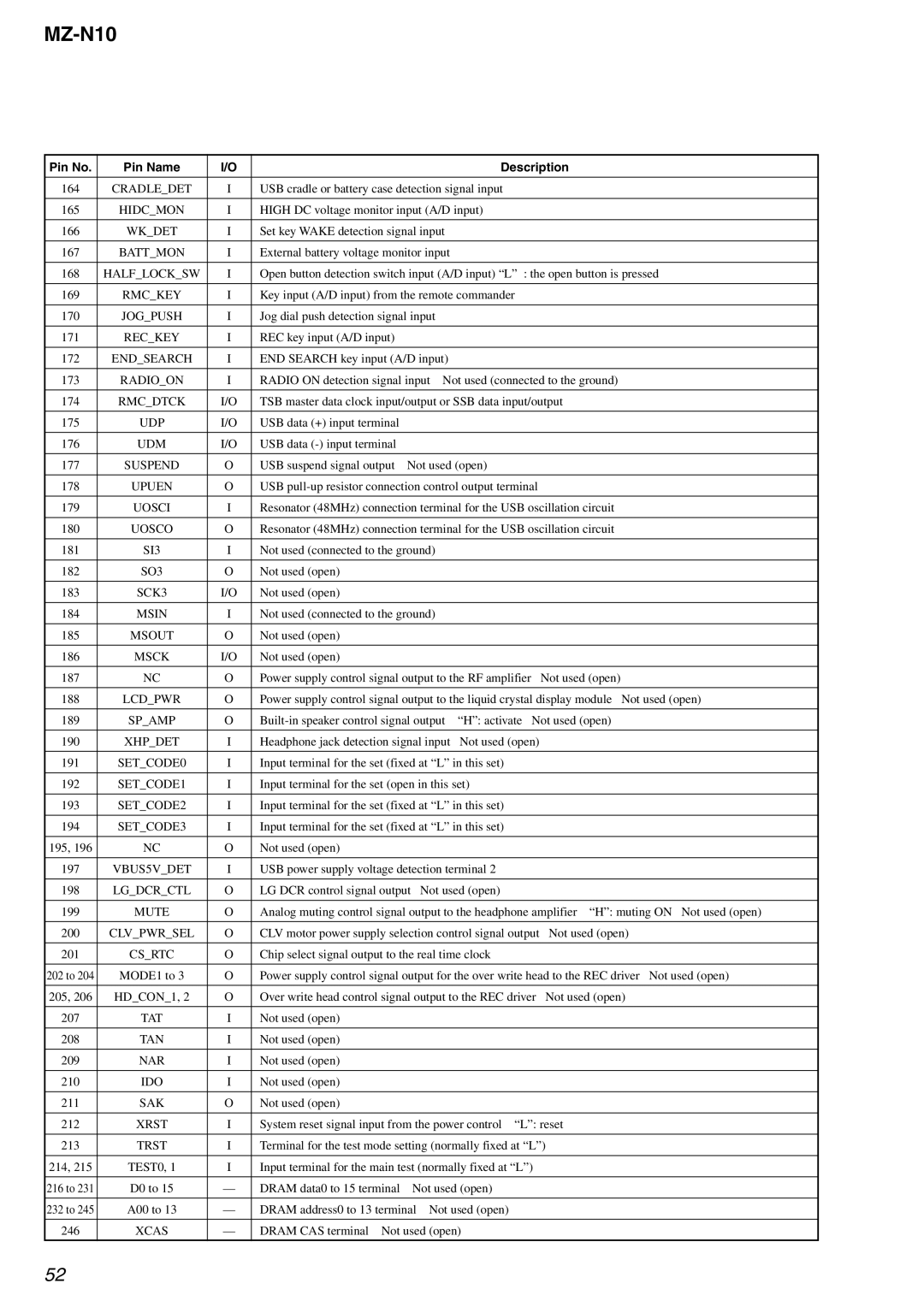
164 | CRADLE_DET | I | USB cradle or battery case detection signal input | |||
|
|
|
| |||
165 | HIDC_MON | I | HIGH DC voltage monitor input (A/D input) | |||
|
|
|
|
| ||
166 | WK_DET | I | Set key WAKE detection signal input |
| ||
|
|
|
|
| ||
167 | BATT_MON | I | External battery voltage monitor input |
| ||
|
|
|
| |||
168 | HALF_LOCK_SW | I | Open button detection switch input (A/D input) “L” : the open button is pressed | |||
|
|
|
| |||
169 | RMC_KEY | I | Key input (A/D input) from the remote commander | |||
|
|
|
|
| ||
170 | JOG_PUSH | I | Jog dial push detection signal input |
| ||
|
|
|
|
|
|
|
171 | REC_KEY | I | REC key input (A/D input) |
|
|
|
|
|
|
|
| ||
172 | END_SEARCH | I | END SEARCH key input (A/D input) |
| ||
|
|
|
| |||
173 | RADIO_ON | I | RADIO ON detection signal input Not used (connected to the ground) | |||
|
|
|
| |||
174 | RMC_DTCK | I/O | TSB master data clock input/output or SSB data input/output | |||
|
|
|
|
|
|
|
175 | UDP | I/O | USB data (+) input terminal |
|
|
|
|
|
|
|
|
|
|
176 | UDM | I/O | USB data |
|
|
|
|
|
|
|
| ||
177 | SUSPEND | O | USB suspend signal output | Not used (open) | ||
|
|
|
| |||
178 | UPUEN | O | USB | |||
|
|
|
| |||
179 | UOSCI | I | Resonator (48MHz) connection terminal for the USB oscillation circuit | |||
|
|
|
| |||
180 | UOSCO | O | Resonator (48MHz) connection terminal for the USB oscillation circuit | |||
|
|
|
|
| ||
181 | SI3 | I | Not used (connected to the ground) |
| ||
|
|
|
|
|
|
|
182 | SO3 | O | Not used (open) |
|
|
|
|
|
|
|
|
|
|
183 | SCK3 | I/O | Not used (open) |
|
|
|
|
|
|
|
| ||
184 | MSIN | I | Not used (connected to the ground) |
| ||
|
|
|
|
|
|
|
185 | MSOUT | O | Not used (open) |
|
|
|
|
|
|
|
|
|
|
186 | MSCK | I/O | Not used (open) |
|
|
|
|
|
|
| |||
187 | NC | O | Power supply control signal output to the RF amplifier Not used (open) | |||
|
|
|
| |||
188 | LCD_PWR | O | Power supply control signal output to the liquid crystal display module Not used (open) | |||
|
|
|
|
| ||
189 | SP_AMP | O | “H”: activate Not used (open) | |||
|
|
|
|
| ||
190 | XHP_DET | I | Headphone jack detection signal input | Not used (open) | ||
|
|
|
| |||
191 | SET_CODE0 | I | Input terminal for the set (fixed at “L” in this set) | |||
|
|
|
| |||
192 | SET_CODE1 | I | Input terminal for the set (open in this set) | |||
|
|
|
| |||
193 | SET_CODE2 | I | Input terminal for the set (fixed at “L” in this set) | |||
|
|
|
| |||
194 | SET_CODE3 | I | Input terminal for the set (fixed at “L” in this set) | |||
|
|
|
|
|
|
|
195, 196 | NC | O | Not used (open) |
|
|
|
|
|
|
| |||
197 | VBUS5V_DET | I | USB power supply voltage detection terminal 2 | |||
|
|
|
|
| ||
198 | LG_DCR_CTL | O | LG DCR control signal output | Not used (open) | ||
|
|
|
| |||
199 | MUTE | O | Analog muting control signal output to the headphone amplifier “H”: muting ON Not used (open) | |||
|
|
|
| |||
200 | CLV_PWR_SEL | O | CLV motor power supply selection control signal output Not used (open) | |||
|
|
|
| |||
201 | CS_RTC | O | Chip select signal output to the real time clock | |||
|
|
|
| |||
202 to 204 | MODE1 to 3 | O | Power supply control signal output for the over write head to the REC driver Not used (open) | |||
|
|
|
| |||
205, 206 | HD_CON_1, 2 | O | Over write head control signal output to the REC driver Not used (open) | |||
|
|
|
|
|
|
|
207 | TAT | I | Not used (open) |
|
|
|
|
|
|
|
|
|
|
208 | TAN | I | Not used (open) |
|
|
|
|
|
|
|
|
|
|
209 | NAR | I | Not used (open) |
|
|
|
|
|
|
|
|
|
|
210 | IDO | I | Not used (open) |
|
|
|
|
|
|
|
|
|
|
211 | SAK | O | Not used (open) |
|
|
|
|
|
|
| |||
212 | XRST | I | System reset signal input from the power control “L”: reset | |||
|
|
|
| |||
213 | TRST | I | Terminal for the test mode setting (normally fixed at “L”) | |||
|
|
|
| |||
214, 215 | TEST0, 1 | I | Input terminal for the main test (normally fixed at “L”) | |||
|
|
|
|
| ||
216 to 231 | D0 to 15 | — | DRAM data0 to 15 terminal | Not used (open) | ||
|
|
|
|
| ||
232 to 245 | A00 to 13 | — | DRAM address0 to 13 terminal | Not used (open) | ||
|
|
|
| |||
246 | XCAS | — | DRAM CAS terminal Not used (open) | |||
|
|
|
|
|
|
|
52