7.2 Drive circuit
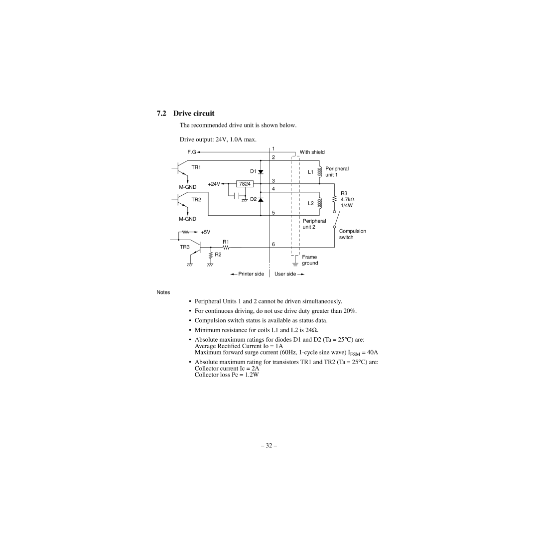
The recommended drive unit is shown below.
Drive output: 24V, 1.0A max.
F.G![]()
1
2
With shield |
TR1
D1 ![]()
L1 | Peripheral | |
unit 1 | ||
|
+24V![]()
7824
3
4
TR2
D2 ![]()
5
| R3 | |
L2 | 4.7kΩ | |
1/4W | ||
|
Peripheral unit 2
| +5V |
|
TR3 | R1 | 6 |
| ||
|
| |
| R2 |
|
Compulsion switch
Frame ground
Printer side | User side |
Notes
•Peripheral Units 1 and 2 cannot be driven simultaneously.
•For continuous driving, do not use drive duty greater than 20%.
•Compulsion switch status is available as status data.
•Minimum resistance for coils L1 and L2 is 24Ω .
•Absolute maximum ratings for diodes D1 and D2 (Ta = 25° C) are: Average Rectified Current Io = 1A
Maximum forward surge current (60Hz,
•Absolute maximum rating for transistors TR1 and TR2 (Ta = 25° C) are: Collector current Ic = 2A
Collector loss Pc = 1.2W
– 32 –