CC2420
|
|
|
|
|
|
|
|
| d |
|
|
|
|
|
|
|
| n | |
|
|
|
|
|
|
| a |
| |
|
|
|
|
|
|
| m |
|
|
|
|
|
|
|
| m |
|
| |
|
|
|
|
| o |
|
|
| |
|
|
| N | c |
|
|
|
| |
|
|
|
|
|
|
|
| ||
|
| O |
| e |
|
|
|
| |
| X |
|
|
|
|
|
| ||
T |
|
| b |
|
|
|
| ||
S |
|
| o |
|
|
|
|
| |
|
| tr |
|
|
|
|
|
| |
| s |
|
|
|
|
|
|
| |
Data transmitted over RF
SFD Pin
|
|
|
|
|
|
|
| d |
|
|
|
|
|
|
|
| te |
| |
|
|
|
|
|
|
| it |
|
|
|
|
|
|
|
| m |
|
| |
|
|
|
|
| s |
|
| ||
|
|
|
| n |
|
|
|
| |
|
|
| a |
|
|
|
|
| |
|
|
| tr |
|
|
|
|
|
|
|
|
| D |
|
|
|
|
|
|
|
| F |
|
|
|
|
|
| |
| S |
|
|
|
|
|
|
| |
|
|
|
|
|
| ||||
Preamble | SFD | Length |
|
| MAC Protocol Data Unit (MPDU) | ||||
|
|
|
|
|
|
|
|
|
|
|
|
|
|
|
|
|
|
|
|
| r |
|
|
|
|
|
|
|
|
|
|
| o |
|
|
|
|
|
|
|
|
|
|
| d |
|
|
|
|
|
|
| U |
| te | ||
|
|
|
|
|
|
|
| it |
| ||
|
|
|
|
|
| D |
| m | w | ||
|
|
|
|
| P |
|
| s | f | ||
|
|
| M |
|
| n |
|
| |||
|
| t |
|
| a |
|
| r |
| ||
| s |
|
| tr |
|
| e |
| |||
a |
| te |
|
|
|
| |||||
L |
|
|
|
| d |
|
| ||||
|
| y |
|
| n |
|
|
| |||
|
| X | u |
|
|
|
| ||||
| b |
|
|
|
|
|
|
|
| ||
|
|
|
| T |
|
|
|
|
|
| |
12 symbol periods | Automatically generated | Data fetched | CRC generated |
by CC2420 | |||
| preamble and SFD | from TXFIFO |
|
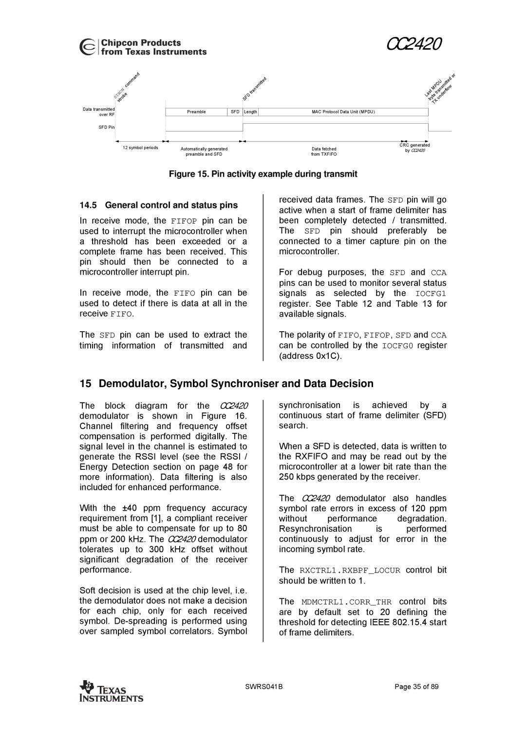
Figure 15. Pin activity example during transmit
14.5 General control and status pins
In receive mode, the FIFOP pin can be used to interrupt the microcontroller when a threshold has been exceeded or a complete frame has been received. This pin should then be connected to a microcontroller interrupt pin.
In receive mode, the FIFO pin can be used to detect if there is data at all in the receive FIFO.
The SFD pin can be used to extract the timing information of transmitted and
received data frames. The SFD pin will go active when a start of frame delimiter has been completely detected / transmitted. The SFD pin should preferably be connected to a timer capture pin on the microcontroller.
For debug purposes, the SFD and CCA pins can be used to monitor several status signals as selected by the IOCFG1 register. See Table 12 and Table 13 for available signals.
The polarity of FIFO, FIFOP, SFD and CCA can be controlled by the IOCFG0 register (address 0x1C).
15 Demodulator, Symbol Synchroniser and Data Decision
The block diagram for the CC2420 demodulator is shown in Figure 16. Channel filtering and frequency offset compensation is performed digitally. The signal level in the channel is estimated to generate the RSSI level (see the RSSI / Energy Detection section on page 48 for more information). Data filtering is also included for enhanced performance.
With the ±40 ppm frequency accuracy requirement from [1], a compliant receiver must be able to compensate for up to 80 ppm or 200 kHz. The CC2420 demodulator tolerates up to 300 kHz offset without significant degradation of the receiver performance.
Soft decision is used at the chip level, i.e. the demodulator does not make a decision for each chip, only for each received symbol.
synchronisation is achieved by a continuous start of frame delimiter (SFD) search.
When a SFD is detected, data is written to the RXFIFO and may be read out by the microcontroller at a lower bit rate than the 250 kbps generated by the receiver.
The CC2420 demodulator also handles symbol rate errors in excess of 120 ppm
without performance degradation.
Resynchronisation is performed continuously to adjust for error in the incoming symbol rate.
The RXCTRL1.RXBPF_LOCUR control bit should be written to 1.
The MDMCTRL1.CORR_THR control bits are by default set to 20 defining the threshold for detecting IEEE 802.15.4 start of frame delimiters.
SWRS041B | Page 35 of 89 |
