Product Description
Key Features
Applications
Table of contents
RF Data Buffering
Ordering Information General Information
ITU-T
Abbreviations
References
Features
Parameter Min Typ Max Units Condition
Absolute Maximum Ratings
Operating Conditions
Parameter Min Max Units Condition
Parameter Min Typ Max Unit Condition / Note
Electrical Specifications
Overall
Transmit Section
Receive Section
Frequency Synthesizer Section
Rssi / Carrier Sense
If Section
VDD
Digital Inputs/Outputs
Voltage Regulator
Battery Monitor
Power Supply
CC2420
Pin Pin Name Pin type Pin Description
Pin Assignment
Avddadc
Circuit Description
CC2420 simplified block diagram
CC2420
Bias resistor
Power supply decoupling and filtering
Application Circuit
Input / output matching
Description
Overview of external components
Transceiver
Transceiver
Bill of materials for the application circuits
Ieee 802.15.4 Modulation Format
Symbol Chip sequence C0, C1, C2, … , C31
Phase
Configuration Overview
SmartRF Studio user interface
Evaluation Software
Register access
13 4-wire Serial Configuration and Data Interface
Pin configuration
Parameter Symbol Min Max Units Conditions
SPI timing specification Status byte
RAM access
Configuration registers write and read operations via SPI
Address Byte Ordering Name Description
CC2420 RAM Memory Space Fifo access
Multiple SPI access
Microcontroller Interface and Pin Description
Configuration interface
Rxfifo overflow
Receive mode
Pin activity examples during receive
Demodulator, Symbol Synchroniser and Data Decision
Frame Format
Demodulator Simplified Block Diagram
MAC protocol data unit
Transmitted Synchronisation Header Length field
Format of the Frame Control Field FCF Frame check sequence
RF Data Buffering
Buffered transmit mode
Buffered receive mode
Fifop
Unbuffered, serial mode
Acknowledge Frames
Address Recognition
Acknowledge frame format
Radio control state machine
Radio control states
Ieee 802.15.4 Nonce
MAC Security Operations Encryption and Authentication
Keys
Nonce / counter
In-line security operations
CC2420 Security Flag Byte Stand-alone encryption
21.7 CCM
CTR mode encryption / decryption
CBC-MAC
Timing
Linear if and AGC Settings
Mode LMIC Time
Rssi / Energy Detection
RF Level dBm
Link Quality Indication
Value
Frequency and Channel Programming
Clear Channel Assessment
27.1 VCO
Output Power Programming
VCO and PLL Self-Calibration
Voltage Regulator
Voltage regulator, simplified schematic
Battery Monitor
Crystal Oscillator
Unmodulated carrier
Input / Output Matching
Transmitter Test Modes
Crystal oscillator component values
CC2420
Modulated spectrum plot
System Considerations and Guidelines
BER / PER measurements
Battery operated systems
Low-cost systems
Antenna Considerations
PCB Layout Recommendations
CC2420
Address Register Register type Description
Configuration Registers
Saes
Configuration registers overview
XOSC16MBYPASS
Bit Field Name Reset
Main 0x10 Main Control Register
CCAHYST20 CCAMODE10 Autocrc Autoack Preamblelength
MDMCTRL0 0x11 Modem Control Register
Reservedframemode Pancoordinator Adrdecode
RSSIVAL70
MDMCTRL1 0x12- Modem Control Register
Rssi 0x13 Rssi and CCA Status and Control Register
CORRTHR40 Demodavgmode Modulationmode
Txctrl 0x15 Transmit Control Register
Syncword 0x14 Sync Word
RXMIXBUFCUR10
RXCTRL0 0x16 Receive control register
RXCTRL1 0x17 Receive control register
Caldone Calrunning Locklength Lockstatus
Fsctrl 0x18 Frequency Synthesizer Control and Status
SECMODE10
SECCTRL0 0x19 Security Control Register
Battmonok Battmonen Battmonvoltage
Battmon 0x1B Battery Monitor Control register
SECCTRL1 0x1A Security Control Register
Sectxl Secrxl
HSSDSRC20 SFDMUX40 CCAMUX40
IOCFG0 0x1C I/O Configuration Register
IOCFG1 0x1D I/O Configuration Register
Manfidl 0x1E Manufacturer ID, Lower 16 Bit
Fsmtc 0x20 Finite state machine time constants
Manfidh 0x1F Manufacturer ID, Upper 16 Bit
Isused = is * Isandmask + Isormask
Manand 0x21 Manual signal and override register1
Lnamixgainmodeo
Manor 0x22 Manual signal or override register
Agcctrl 0x23 AGC Control
Vgagainoe
AGCTST2 0x26 AGC Test Register
AGCTST0 0x24 AGC Test Register
AGCTST1 0x25 AGC Test Register
FSTST2 0x29 Frequency Synthesizer Test Register
FSTST0 0x27 Frequency Synthesizer Test Register
FSTST1 0x28 Frequency Synthesizer Test Register
Fsmstate 0x2C Finite state machine information
FSTST3 0x2A Frequency Synthesizer Test Register
Rxbpftst 0x2B Receiver Bandpass Filters Test Register
Dactst 0x2E DAC Test Register
Adcclockdisable
Adctst 0x2D ADC Test Register
Rxfifo 0x3F Receive Fifo Byte register
Oscillator must be running for accessing the Rxfifo
Toptst 0x2F Top Level Test Register
Txfifo 0x3E Transmit Fifo Byte register
Signal output on CCA pin Description
Test Output Signals
CCA test signal select table
Signal output on SFD pin Description
SFD test signal select table
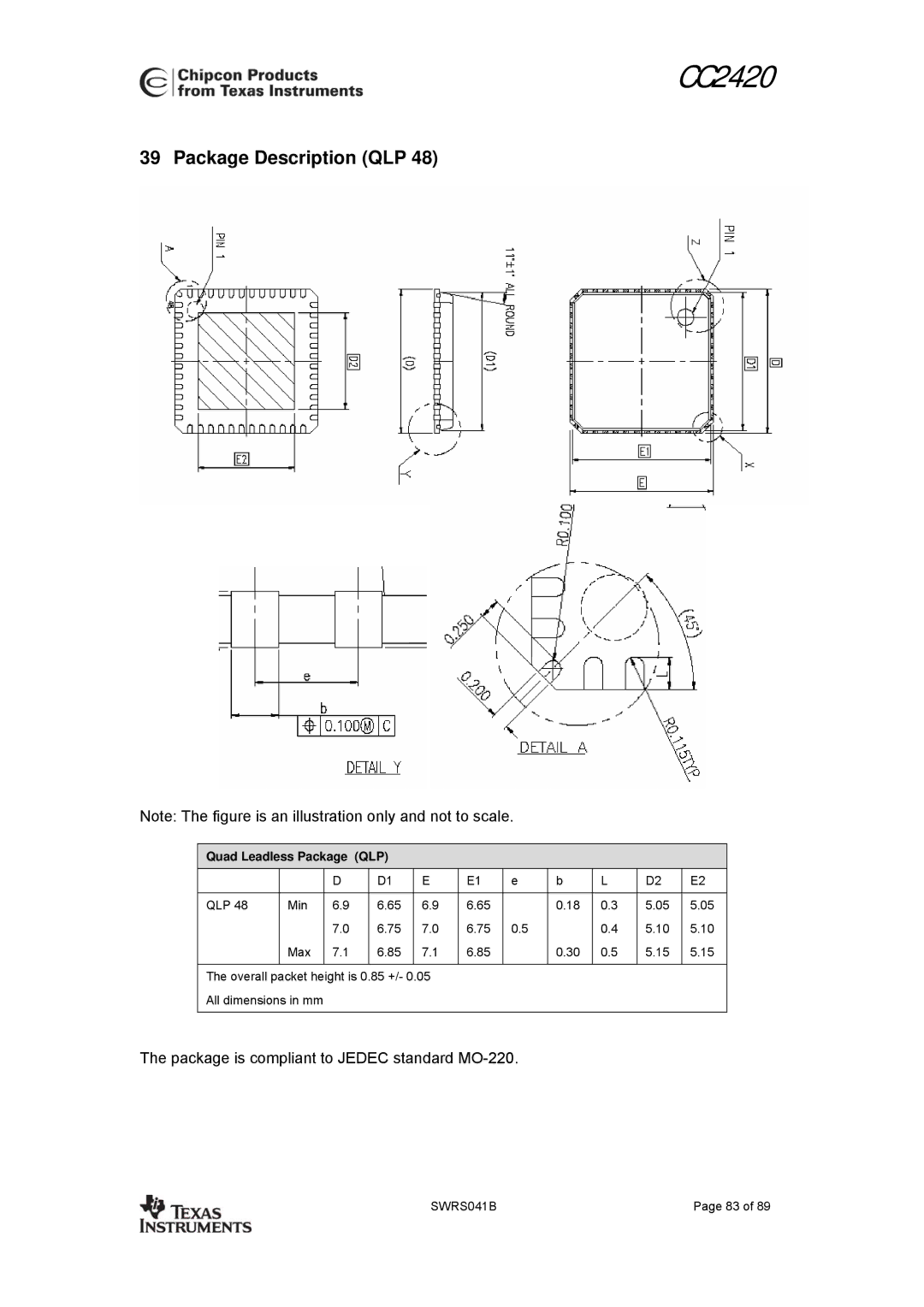
Quad Leadless Package QLP
Package Description QLP
Thermal resistance
Recommended layout for package QLP
Package thermal properties
Soldering information
Tape and Reel Specification
40.3 Plastic tube specification
40.4 Carrier tape and reel specification
Tube Specification
Revision Date Description/Changes
General Information
42.1 Document History
Product Status Definitions
Data Sheet Identification Product Status Definition
Product Information Centers
Address Information
TI Worldwide Technical Support Internet
2007, Texas Instruments. All rights reserved
Important Notice