www.ti.com
EDMA BUS
Peripheral Architecture
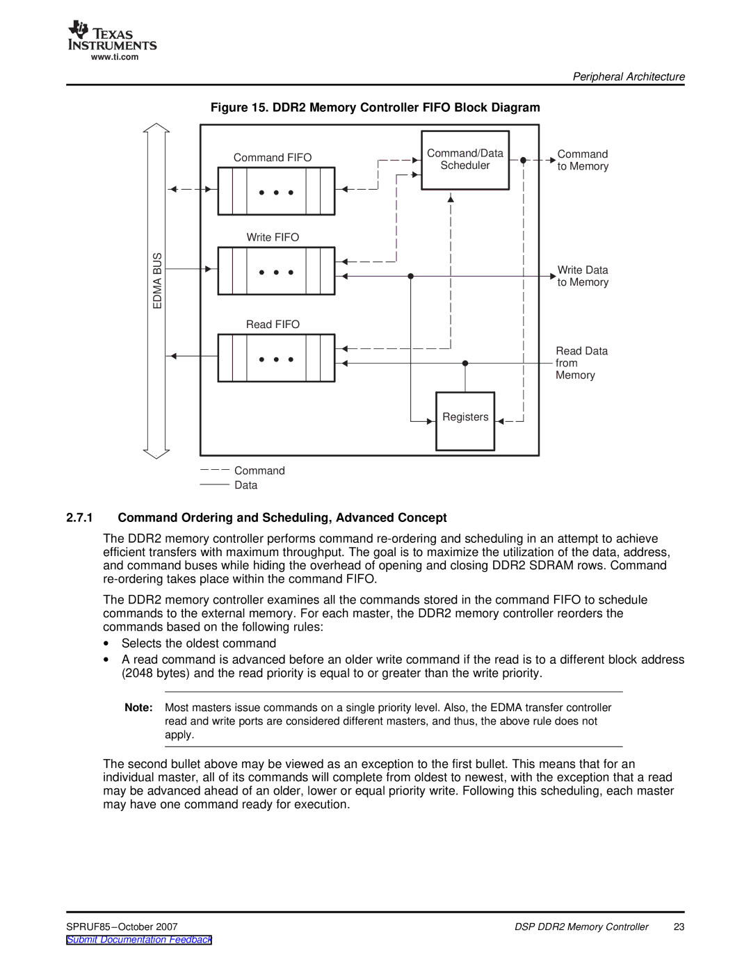
Figure 15. DDR2 Memory Controller FIFO Block Diagram
Command FIFO | Command/Data | Command | |
Scheduler | to Memory | ||
| |||
Write FIFO |
|
| |
|
| Write Data | |
|
| to Memory | |
Read FIFO |
|
| |
|
| Read Data | |
|
| from | |
|
| Memory | |
| Registers |
| |
Command |
|
| |
Data |
|
|
2.7.1Command Ordering and Scheduling, Advanced Concept
The DDR2 memory controller performs command
The DDR2 memory controller examines all the commands stored in the command FIFO to schedule commands to the external memory. For each master, the DDR2 memory controller reorders the commands based on the following rules:
∙Selects the oldest command
∙A read command is advanced before an older write command if the read is to a different block address (2048 bytes) and the read priority is equal to or greater than the write priority.
Note: Most masters issue commands on a single priority level. Also, the EDMA transfer controller read and write ports are considered different masters, and thus, the above rule does not apply.
The second bullet above may be viewed as an exception to the first bullet. This means that for an individual master, all of its commands will complete from oldest to newest, with the exception that a read may be advanced ahead of an older, lower or equal priority write. Following this scheduling, each master may have one command ready for execution.
SPRUF85 | DSP DDR2 Memory Controller | 23 |