www.ti.com
Peripheral Architecture
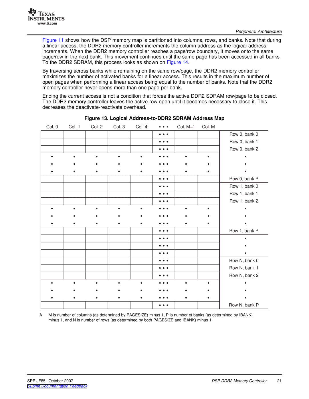
Figure 11 shows how the DSP memory map is partitioned into columns, rows, and banks. Note that during a linear access, the DDR2 memory controller increments the column address as the logical address increments. When the DDR2 memory controller reaches a page/row boundary, it moves onto the same page/row in the next bank. This movement continues until the same page has been accessed in all banks. To the DDR2 SDRAM, this process looks as shown on Figure 14.
By traversing across banks while remaining on the same row/page, the DDR2 memory controller maximizes the number of activated banks for a linear access. This results in the maximum number of open pages when performing a linear access being equal to the number of banks. Note that the DDR2 memory controller never opens more than one page per bank.
Ending the current access is not a condition that forces the active DDR2 SDRAM row/page to be closed. The DDR2 memory controller leaves the active row open until it becomes necessary to close it. This decreases the deactivate-reactivate overhead.
Figure 13. Logical Address-to-DDR2 SDRAM Address Map
Col. 0 | Col. 1 | Col. 2 | Col. 3 | Col. 4 | Col. M−1 | Col. M |
Row 0, bank 0
Row 0, bank 1
Row 0, bank 2
Row 0, bank P
Row 1, bank 0
Row 1, bank 1
Row 1, bank 2
Row 1, bank P
Row N, bank 0
Row N, bank 1
Row N, bank 2
Row N, bank P
AM is number of columns (as determined by PAGESIZE) minus 1, P is number of banks (as determined by IBANK) minus 1, and N is number of rows (as determined by both PAGESIZE and IBANK) minus 1.
SPRUF85 | DSP DDR2 Memory Controller | 21 |
Submit Documentation Feedback |
|
|