www.ti.com
|
|
| DDR2 Memory Controller Registers |
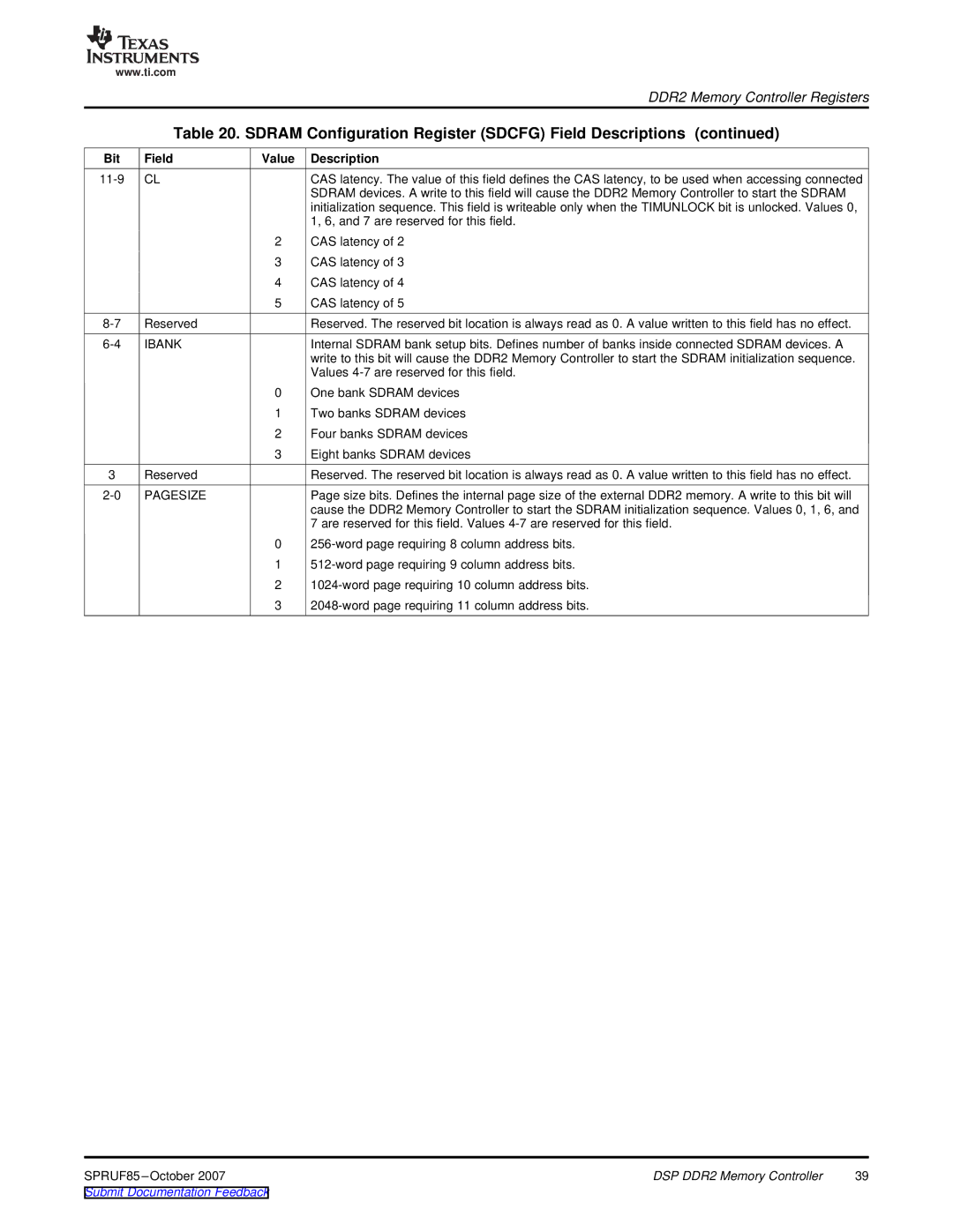
| Table 20. SDRAM Configuration Register (SDCFG) Field Descriptions (continued) | ||
Bit | Field | Value | Description |
CL |
| CAS latency. The value of this field defines the CAS latency, to be used when accessing connected | |
|
|
| SDRAM devices. A write to this field will cause the DDR2 Memory Controller to start the SDRAM |
|
|
| initialization sequence. This field is writeable only when the TIMUNLOCK bit is unlocked. Values 0, |
|
|
| 1, 6, and 7 are reserved for this field. |
|
| 2 | CAS latency of 2 |
|
| 3 | CAS latency of 3 |
|
| 4 | CAS latency of 4 |
|
| 5 | CAS latency of 5 |
Reserved |
| Reserved. The reserved bit location is always read as 0. A value written to this field has no effect. | |
IBANK |
| Internal SDRAM bank setup bits. Defines number of banks inside connected SDRAM devices. A | |
|
|
| write to this bit will cause the DDR2 Memory Controller to start the SDRAM initialization sequence. |
|
|
| Values |
|
| 0 | One bank SDRAM devices |
|
| 1 | Two banks SDRAM devices |
|
| 2 | Four banks SDRAM devices |
|
| 3 | Eight banks SDRAM devices |
3 | Reserved |
| Reserved. The reserved bit location is always read as 0. A value written to this field has no effect. |
PAGESIZE |
| Page size bits. Defines the internal page size of the external DDR2 memory. A write to this bit will | |
|
|
| cause the DDR2 Memory Controller to start the SDRAM initialization sequence. Values 0, 1, 6, and |
|
|
| 7 are reserved for this field. Values |
|
| 0 | |
|
| 1 | |
|
| 2 | |
|
| 3 | |
SPRUF85 | DSP DDR2 Memory Controller | 39 |
Submit Documentation Feedback |
|
|