www.ti.com
Peripheral Architecture
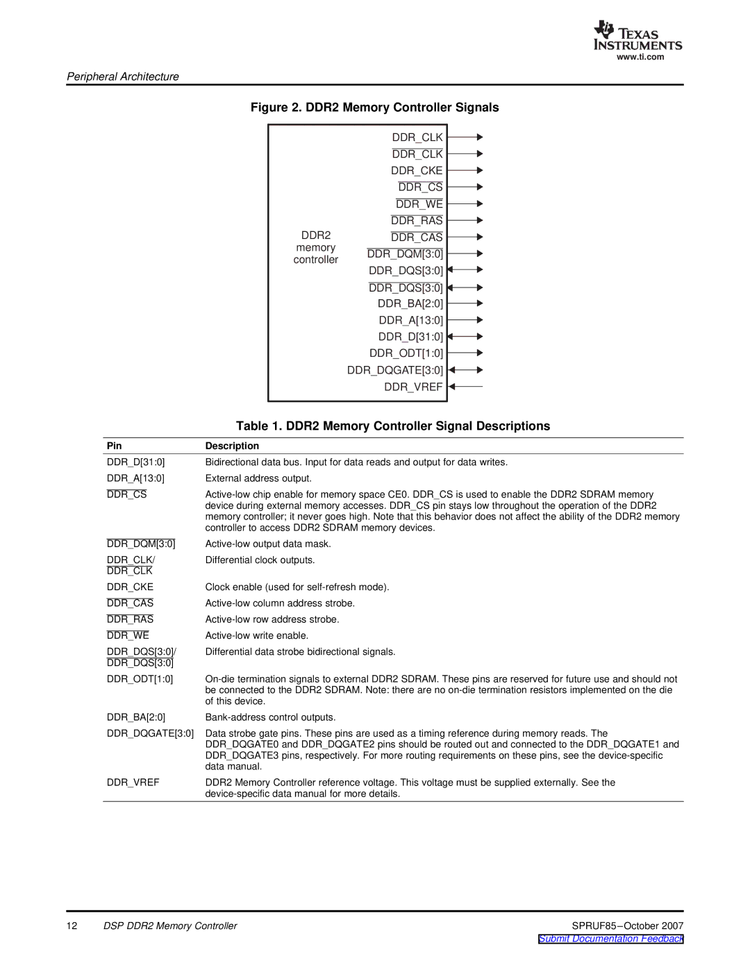
Figure 2. DDR2 Memory Controller Signals
DDR_CLK ![]()
DDR_CLK ![]()
DDR_CKE ![]()
DDR_CS ![]()
DDR_WE ![]()
DDR_RAS ![]()
DDR2DDR_CAS ![]() memory
memory
controller DDR_DQM[3:0] DDR_DQS[3:0] ![]()
![]()
DDR_DQS[3:0] ![]()
![]()
DDR_BA[2:0] ![]()
DDR_A[13:0] ![]()
DDR_D[31:0] ![]()
![]()
DDR_ODT[1:0] ![]()
DDR_DQGATE[3:0] ![]()
DDR_VREF ![]()
| Table 1. DDR2 Memory Controller Signal Descriptions |
Pin | Description |
DDR_D[31:0] | Bidirectional data bus. Input for data reads and output for data writes. |
DDR_A[13:0] | External address output. |
DDR_CS | |
| device during external memory accesses. DDR_CS pin stays low throughout the operation of the DDR2 |
| memory controller; it never goes high. Note that this behavior does not affect the ability of the DDR2 memory |
| controller to access DDR2 SDRAM memory devices. |
DDR_DQM[3:0] | |
DDR_CLK/ | Differential clock outputs. |
DDR_CLK |
|
DDR_CKE | Clock enable (used for |
DDR_CAS | |
DDR_RAS | |
DDR_WE | |
DDR_DQS[3:0]/ | Differential data strobe bidirectional signals. |
DDR_DQS[3:0] |
|
DDR_ODT[1:0] | |
| be connected to the DDR2 SDRAM. Note: there are no |
| of this device. |
DDR_BA[2:0] | |
DDR_DQGATE[3:0] | Data strobe gate pins. These pins are used as a timing reference during memory reads. The |
| DDR_DQGATE0 and DDR_DQGATE2 pins should be routed out and connected to the DDR_DQGATE1 and |
| DDR_DQGATE3 pins, respectively. For more routing requirements on these pins, see the |
| data manual. |
DDR_VREF | DDR2 Memory Controller reference voltage. This voltage must be supplied externally. See the |
|
12 | DSP DDR2 Memory Controller | SPRUF85 |