www.ti.com
Peripheral Architecture
2.11 DDR2 SDRAM Memory Initialization
DDR2 SDRAM devices contain mode and extended mode registers that configure the mode of operation for the device. These registers control parameters such as burst type, burst length, and CAS latency. The DDR2 memory controller programs the mode and extended mode registers of the DDR2 memory by issuing MRS and EMRS commands during the initialization sequence described in Section 2.11.2 and Section 2.11.3. The initialization sequence performed by the DDR2 memory controller is compliant with the
The DDR2 memory controller performs the initialization sequence under the following conditions:
∙Automatically following a hard or soft reset, see Section 2.11.2.
∙Following a write to the two
At the end of the initialization sequence, the DDR2 memory controller performs an
When the initialization section is started automatically after a hard or soft reset, commands and data stored in the DDR2 memory controller FIFOs are lost. However, when the initialization sequence is initiated by a write to the two
2.11.1DDR2 SDRAM Device Mode Register Configuration Values
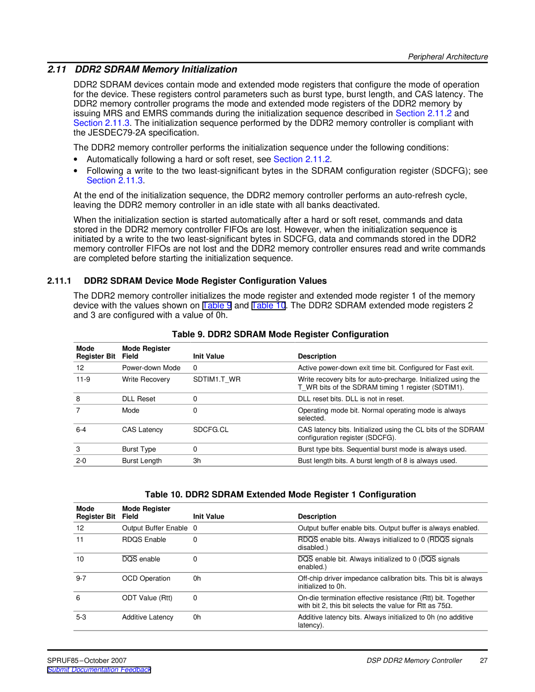
The DDR2 memory controller initializes the mode register and extended mode register 1 of the memory device with the values shown on Table 9 and Table 10. The DDR2 SDRAM extended mode registers 2 and 3 are configured with a value of 0h.
Table 9. DDR2 SDRAM Mode Register Configuration
Mode | Mode Register |
|
|
Register Bit | Field | Init Value | Description |
12 | 0 | Active | |
Write Recovery | SDTIM1.T_WR | Write recovery bits for | |
|
|
| T_WR bits of the SDRAM timing 1 register (SDTIM1). |
8 | DLL Reset | 0 | DLL reset bits. DLL is not in reset. |
7 | Mode | 0 | Operating mode bit. Normal operating mode is always |
|
|
| selected. |
CAS Latency | SDCFG.CL | CAS latency bits. Initialized using the CL bits of the SDRAM | |
|
|
| configuration register (SDCFG). |
3 | Burst Type | 0 | Burst type bits. Sequential burst mode is always used. |
Burst Length | 3h | Bust length bits. A burst length of 8 is always used. |
Table 10. DDR2 SDRAM Extended Mode Register 1 Configuration
Mode | Mode Register |
|
|
|
Register Bit | Field | Init Value | Description |
|
12 | Output Buffer Enable | 0 | Output buffer enable bits. Output buffer is always enabled. |
|
11 | RDQS Enable | 0 | RDQS enable bits. Always initialized to 0 (RDQS signals |
|
|
|
| disabled.) |
|
10 | DQS enable | 0 | DQS enable bit. Always initialized to 0 (DQS signals |
|
|
|
| enabled.) |
|
OCD Operation | 0h | |||
|
|
| initialized to 0h. |
|
6 | ODT Value (Rtt) | 0 |
| |
|
|
| with bit 2, this bit selects the value for Rtt as 75Ω. |
|
Additive Latency | 0h | Additive latency bits. Always initialized to 0h (no additive |
| |
|
|
| latency). |
|
SPRUF85 |
| DSP DDR2 Memory Controller | 27 | |
Submit Documentation Feedback |
|
|
| |
