www.ti.com
DDR2 Memory Controller Registers
4.1Module ID and Revision Register (MIDR)
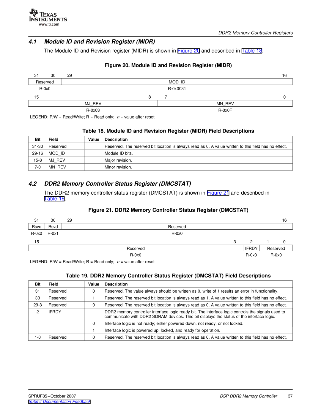
The Module ID and Revision register (MIDR) is shown in Figure 20 and described in Table 18.
Figure 20. Module ID and Revision Register (MIDR)
31 | 30 | 29 |
| 16 |
Reserved |
|
| MOD_ID | |
|
|
| ||
15 |
| 8 | 7 | 0 |
|
| MJ_REV |
| MN_REV |
|
|
| ||
LEGEND: R/W = Read/Write; R = Read only; |
|
| ||
|
| Table 18. Module ID and Revision Register (MIDR) Field Descriptions |
Bit | Field | Value Description |
Reserved | Reserved. The reserved bit location is always read as 0. A value written to this field has no effect. | |
MOD_ID | Module ID bits. | |
MJ_REV | Major revision. | |
MN_REV | Minor revision. |
4.2DDR2 Memory Controller Status Register (DMCSTAT)
The DDR2 memory controller status register (DMCSTAT) is shown in Figure 21 and described in Table 19.
Figure 21. DDR2 Memory Controller Status Register (DMCSTAT)
31 | 30 | 29 |
|
|
| 16 |
Rsvd | Rsvd |
| Reserved |
|
|
|
|
|
|
| |||
15 |
|
| 3 | 2 | 1 | 0 |
|
| Reserved |
| IFRDY | Reserved | |
|
|
|
| |||
LEGEND: R/W = Read/Write; R = Read only; |
|
|
|
| ||
Table 19. DDR2 Memory Controller Status Register (DMCSTAT) Field Descriptions
Bit | Field | Value | Description |
31 | Reserved | 0 | Reserved. The value always should be written as 0. write of 1 results an error in functionality. |
30 | Reserved | 1 | Reserved. The reserved bit location is always read as 1. A value written to this field has no effect. |
Reserved | 0 | Reserved. The reserved bit location is always read as 0. A value written to this field has no effect. | |
2 | IFRDY |
| DDR2 memory controller interface logic ready bit. The interface logic controls the signals used to |
|
|
| communicate with DDR2 SDRAM devices. This bit displays the status of the interface logic. |
|
| 0 | Interface logic is not ready; either powered down, not ready, or not locked. |
|
| 1 | Interface logic is powered up, locked, and ready for operation. |
Reserved | 0 | Reserved. The reserved bit location is always read as 0. A value written to this field has no effect. |
SPRUF85 | DSP DDR2 Memory Controller | 37 |
Submit Documentation Feedback |
|
|
