
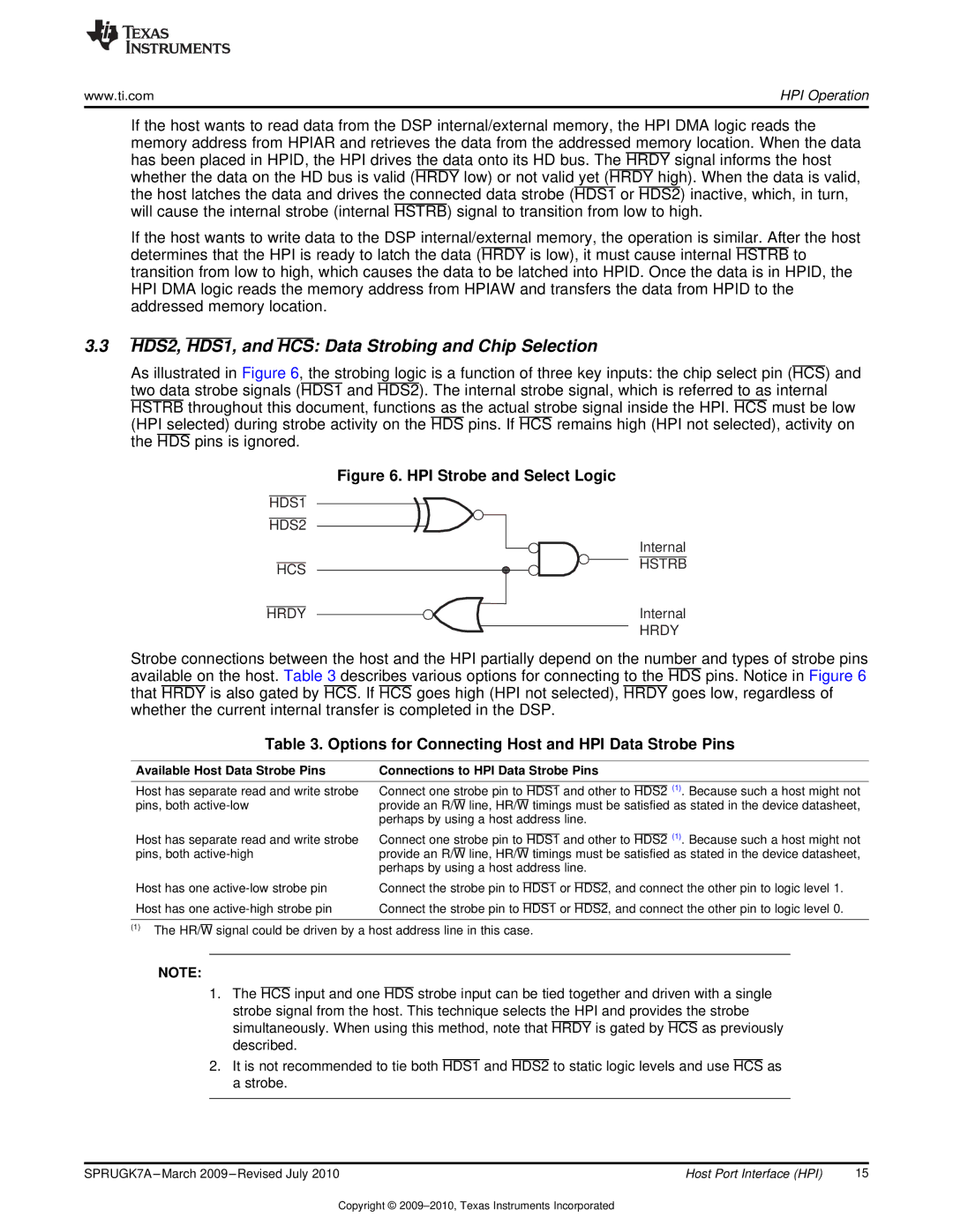
TMS320C6457 specifications
The Texas Instruments TMS320C6457 is a high-performance digital signal processor (DSP) designed for demanding applications in telecommunications, industrial control, and video processing. As part of the TMS320C6000 family, the C6457 combines advanced features with impressive processing capabilities, making it a popular choice among developers looking for efficient and robust solutions.One of the key features of the TMS320C6457 is its architecture, which is based on the super Harvard architecture. This design separates program and data memory paths, allowing for parallel instruction execution. The C6457 operates at clock speeds of up to 1 GHz, enabling it to deliver peak performance of over 6,000 MIPS (Million Instructions Per Second) and 12,000 MADDs (Multiply-Accumulate operations per second). Such high throughput makes the C6457 suitable for real-time processing applications that require rapid data handling.
The C6457 DSP integrates a rich set of on-chip resources, including up to 1MB of on-chip SRAM, which serves as a fast cache for data and instructions. The device features multiple high-speed interfaces, such as 10/100/1000 Ethernet, Serial RapidIO, and PCI-Express, facilitating seamless connectivity with other devices and systems. Furthermore, the TMS320C6457 supports various communication protocols, allowing it to adapt to a wide range of application scenarios.
In terms of power efficiency, the TMS320C6457 is designed with sophisticated power management features. It includes dynamic voltage and frequency scaling, which adjust power consumption based on workload requirements without compromising performance. This capability is particularly valuable in battery-operated devices or environments where thermal management is critical.
The TMS320C6457 also benefits from extensive software support, including the Texas Instruments DSP/BIOS real-time operating system and Code Composer Studio integrated development environment. Developers can leverage these tools for efficient code development, debugging, and system optimization. Additionally, Texas Instruments provides a range of libraries and algorithms optimized for the C6457, facilitating rapid application development.
Overall, the Texas Instruments TMS320C6457 DSP stands out due to its robust architecture, high processing capabilities, comprehensive connectivity options, and power management features. These attributes make it a versatile solution for a broad spectrum of applications in digital signal processing, where performance and efficiency are paramount. As technology continues to advance, the TMS320C6457 remains a relevant and potent option for developers seeking to push the boundaries of digital signal processing.