www.ti.com
Peripheral Architecture
2.4.6Write (WRT) Command
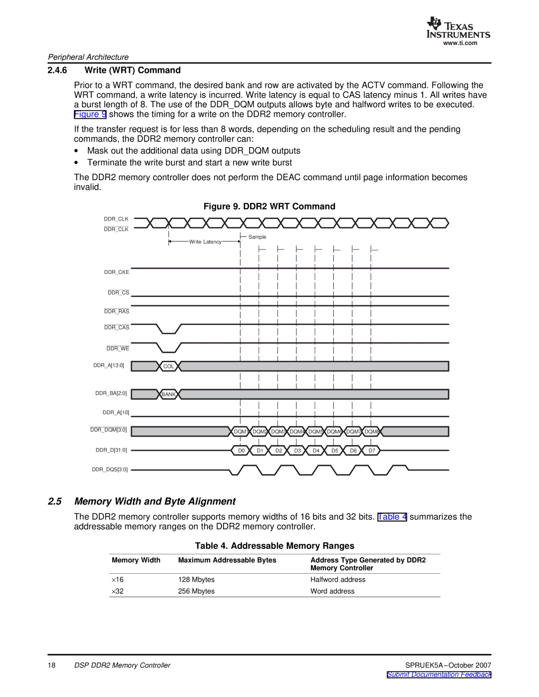
Prior to a WRT command, the desired bank and row are activated by the ACTV command. Following the WRT command, a write latency is incurred. Write latency is equal to CAS latency minus 1. All writes have a burst length of 8. The use of the DDR_DQM outputs allows byte and halfword writes to be executed.
Figure 9 shows the timing for a write on the DDR2 memory controller.
If the transfer request is for less than 8 words, depending on the scheduling result and the pending commands, the DDR2 memory controller can:
∙Mask out the additional data using DDR_DQM outputs
∙Terminate the write burst and start a new write burst
The DDR2 memory controller does not perform the DEAC command until page information becomes invalid.
Figure 9. DDR2 WRT Command
DDR_CLK
DDR_CLK
Sample
Write Latency
DDR_CKE
DDR_CS
DDR_RAS
DDR_CAS
DDR_WE
DDR_A[13:0] ![]() COL
COL ![]()
DDR_BA[2:0] | BANK |
|
|
|
|
|
|
|
DDR_A[10] |
|
|
|
|
|
|
|
|
DDR_DQM[3:0] | DQM1 DQM2 DQM3 DQM4 DQM5 DQM6 DQM7 DQM8 | |||||||
| ||||||||
DDR_D[31:0] | D0 | D1 | D2 | D3 | D4 | D5 | D6 | D7 |
DDR_DQS[3:0] |
|
|
|
|
|
|
|
|
2.5Memory Width and Byte Alignment
The DDR2 memory controller supports memory widths of 16 bits and 32 bits. Table 4 summarizes the addressable memory ranges on the DDR2 memory controller.
Table 4. Addressable Memory Ranges
Memory Width | Maximum Addressable Bytes | Address Type Generated by DDR2 |
|
| Memory Controller |
×16 | 128 Mbytes | Halfword address |
×32 | 256 Mbytes | Word address |
18 | DSP DDR2 Memory Controller | SPRUEK5A |
