www.ti.com
Peripheral Architecture
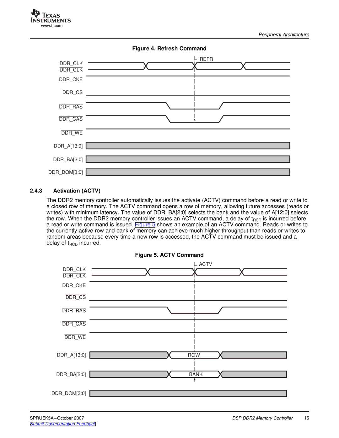
Figure 4. Refresh Command
REFR
DDR_CLK
DDR_CLK
DDR_CKE
DDR_CS
DDR_RAS
DDR_CAS
DDR_WE
DDR_A[13:0]
DDR_BA[2:0]
DDR_DQM[3:0]
2.4.3Activation (ACTV)
The DDR2 memory controller automatically issues the activate (ACTV) command before a read or write to a closed row of memory. The ACTV command opens a row of memory, allowing future accesses (reads or writes) with minimum latency. The value of DDR_BA[2:0] selects the bank and the value of A[12:0] selects the row. When the DDR2 memory controller issues an ACTV command, a delay of tRCD is incurred before a read or write command is issued. Figure 5 shows an example of an ACTV command. Reads or writes to the currently active row and bank of memory can achieve much higher throughput than reads or writes to random areas because every time a new row is accessed, the ACTV command must be issued and a delay of tRCD incurred.
Figure 5. ACTV Command
| DDR_CLK |
|
|
|
|
|
|
|
| ACTV |
| ||||||||||
|
|
|
|
|
|
|
|
|
| ||||||||||||
|
|
|
|
|
|
|
|
|
|
|
|
|
|
|
| ||||||
|
|
|
|
|
|
|
|
|
|
|
|
|
|
|
|
|
|
|
|
|
|
DDR_CLK |
|
|
|
|
|
|
|
|
|
|
|
|
|
|
| ||||||
|
|
|
|
|
|
|
|
|
|
|
|
|
|
| |||||||
DDR_CKE |
|
|
|
|
|
|
|
|
|
|
|
|
|
|
| ||||||
|
|
|
|
|
|
|
|
|
|
|
|
|
|
| |||||||
|
|
|
|
|
|
|
|
|
|
|
|
|
|
|
|
|
|
|
|
| |
|
|
|
| DDR_CS |
|
|
|
|
|
|
|
|
|
|
|
|
|
|
| ||
|
|
|
|
|
|
|
|
|
|
|
|
|
|
|
|
|
|
|
|
|
|
|
|
|
|
|
|
|
|
|
|
|
|
|
|
|
|
|
|
| |||
DDR_RAS |
|
|
|
|
|
|
|
|
|
|
|
|
|
|
| ||||||
|
|
|
|
|
|
|
|
|
|
|
|
|
|
|
|
|
|
|
|
|
|
|
|
|
|
|
|
|
|
|
|
|
|
|
|
|
|
|
| ||||
DDR_CAS |
|
|
|
|
|
|
|
|
|
|
|
|
|
|
| ||||||
|
|
|
|
|
|
|
|
|
|
|
|
|
|
|
|
|
|
|
|
|
|
|
|
|
|
|
|
|
|
|
|
|
|
|
|
|
|
|
|
|
| ||
|
| DDR_WE |
|
|
|
|
|
|
|
|
|
|
|
|
|
|
| ||||
DDR_A[13:0] |
|
|
|
|
|
|
|
|
|
|
|
|
|
|
| ||||||
|
|
|
|
| ROW |
|
|
|
| ||||||||||||
|
|
|
|
|
|
|
|
|
|
|
|
|
|
|
|
| |||||
DDR_BA[2:0] |
|
|
|
|
| BANK |
| ||||||||||||||
DDR_DQM[3:0] |
|
|
|
|
|
|
|
|
|
|
|
|
|
|
| ||||||
|
|
|
|
|
|
|
|
|
|
|
|
|
|
| |||||||
SPRUEK5A |
|
|
|
|
|
|
|
|
|
| DSP DDR2 Memory Controller | 15 | |||||||||
