www.ti.com
Using the DDR2 Memory Controller
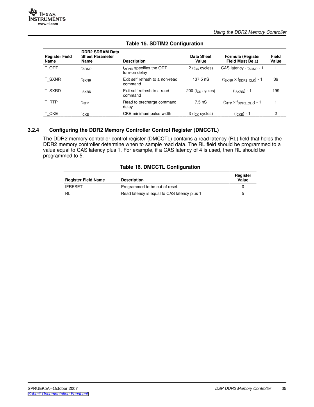
Table 15. SDTIM2 Configuration
| DDR2 SDRAM Data |
|
|
|
|
Register Field | Sheet Parameter |
| Data Sheet | Formula (Register | Field |
Name | Name | Description | Value | Field Must Be ≥) | Value |
T_ODT | tAOND | tAOND specifies the ODT | 2 (tCK cycles) | CAS latency - tAOND - 1 | 1 |
|
|
|
|
| |
T_SXNR | tSXNR | Exit self refresh to a | 137.5 nS | (tSXNR × fDDR2_CLK) - 1 | 36 |
|
| command |
|
|
|
T_SXRD | tSXRD | Exit self refresh to a read | 200 (tCK cycles) | (tSXRD) - 1 | 199 |
|
| command |
|
|
|
T_RTP | tRTP | Read to precharge command | 7.5 nS | (tRTP × fDDR2_CLK) - 1 | 1 |
|
| delay |
|
|
|
T_CKE | tCKE | CKE minimum pulse width | 3 (tCK cycles) | (tCKE) - 1 | 2 |
3.2.4Configuring the DDR2 Memory Controller Control Register (DMCCTL)
The DDR2 memory controller control register (DMCCTL) contains a read latency (RL) field that helps the DDR2 memory controller determine when to sample read data. The RL field should be programmed to a value equal to CAS latency plus 1. For example, if a CAS latency of 4 is used, then RL should be programmed to 5.
Table 16. DMCCTL Configuration
|
| Register |
Register Field Name | Description | Value |
IFRESET | Programmed to be out of reset. | 0 |
RL | Read latency is equal to CAS latency plus 1. | 5 |
SPRUEK5A | DSP DDR2 Memory Controller | 35 |
Submit Documentation Feedback |
|
|