


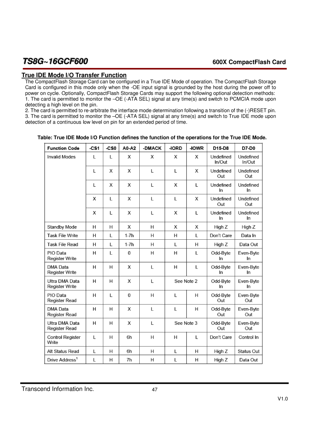
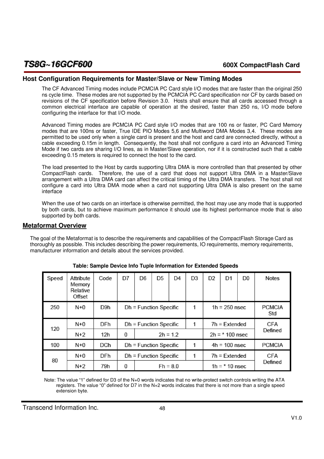
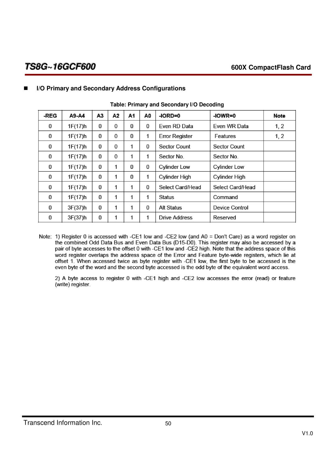

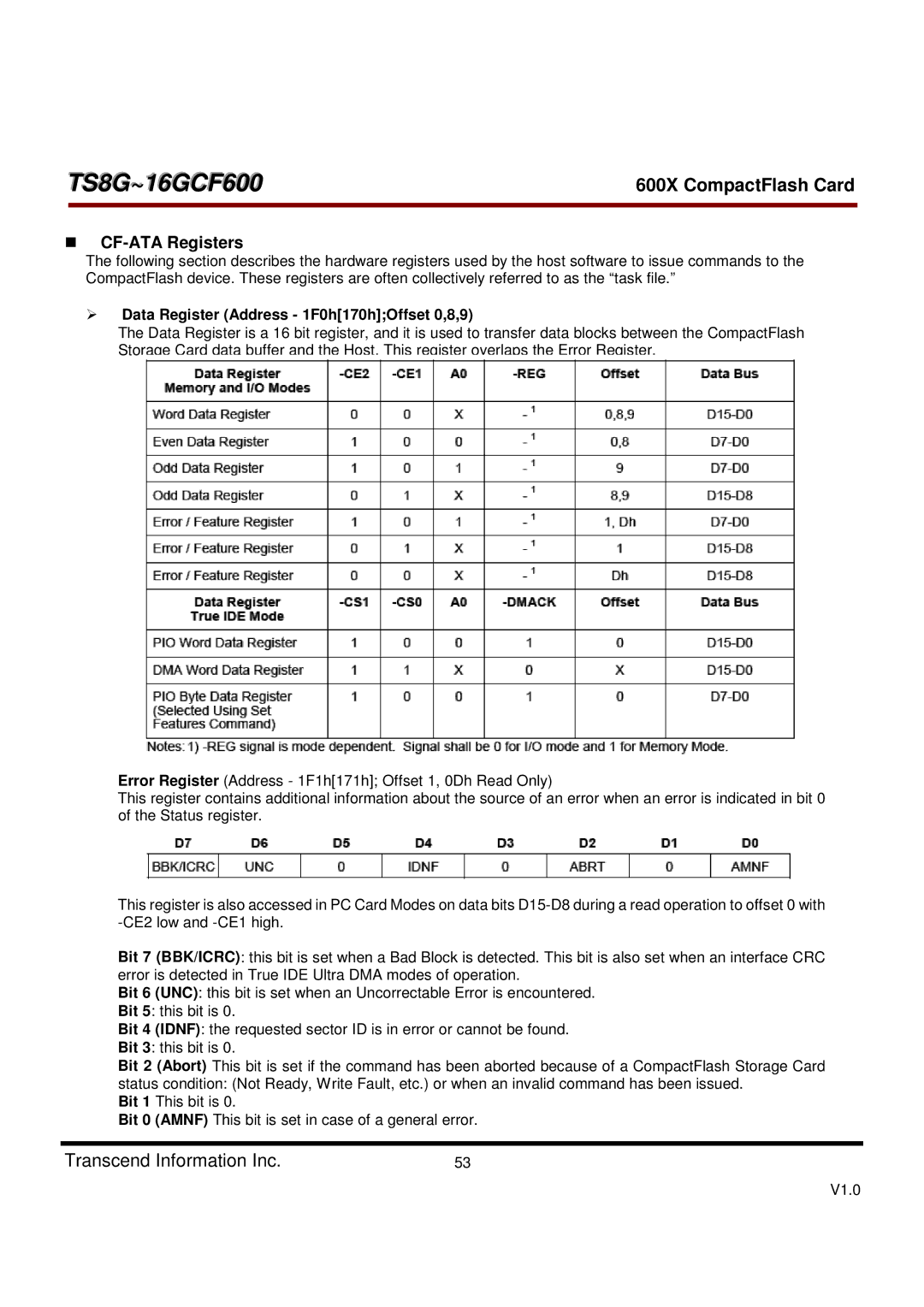

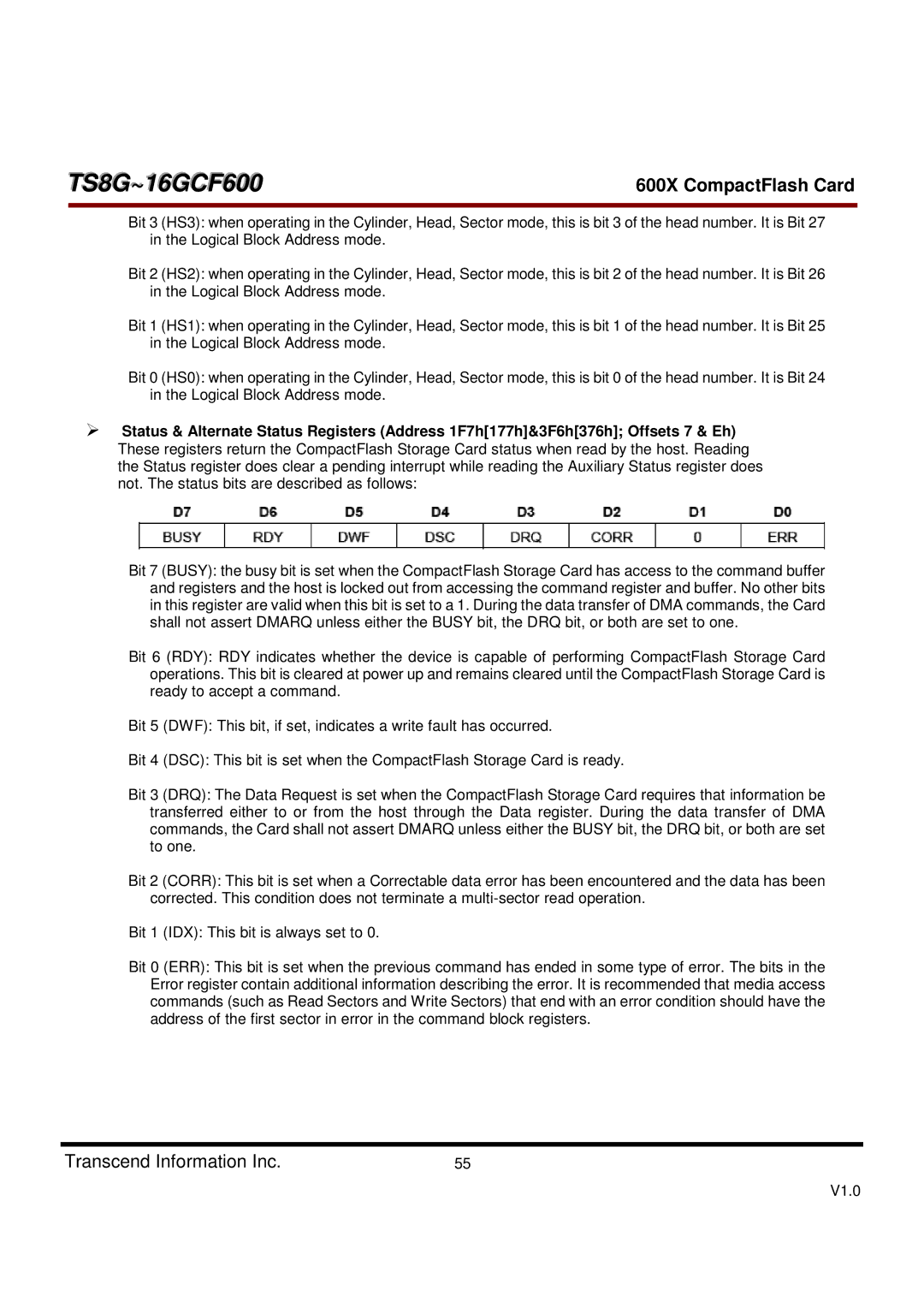


TS8G~16GCF600 |
|
|
|
|
|
|
|
|
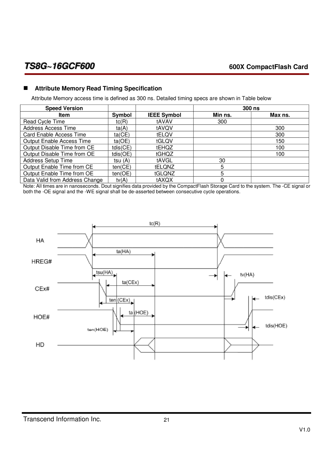
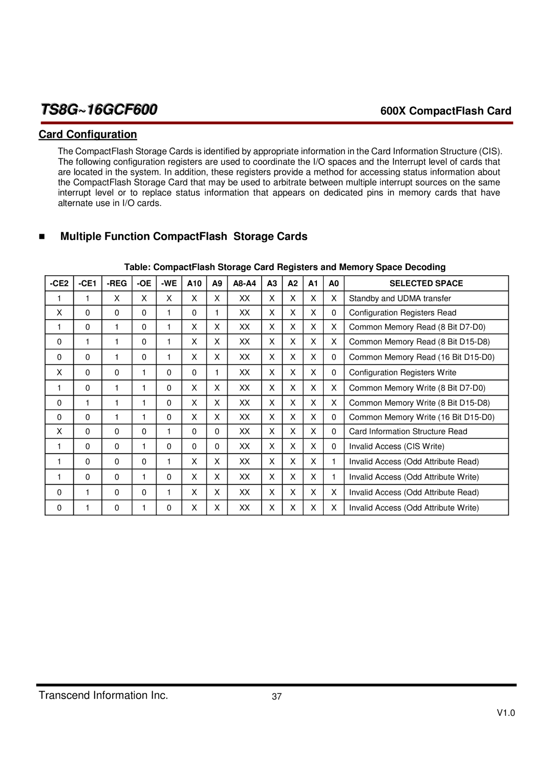
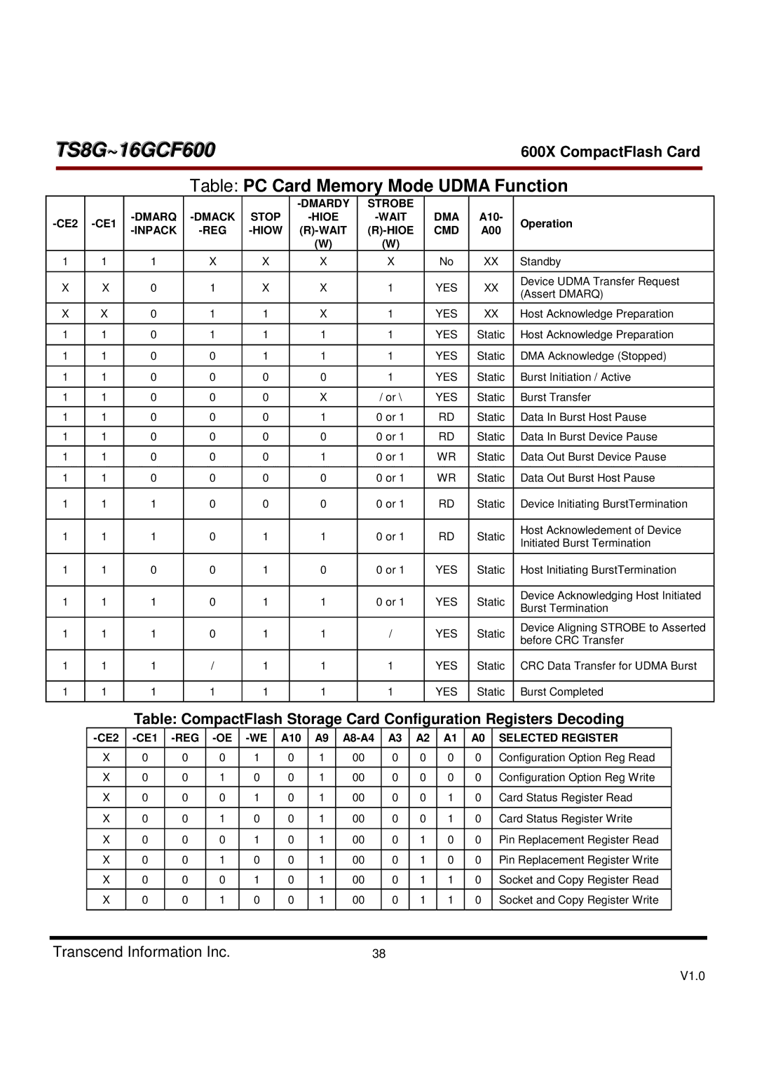
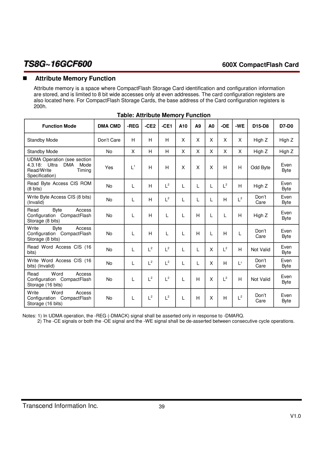
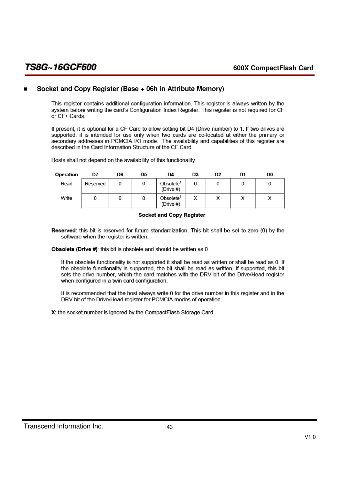
| 600X CompactFlash Card | ||||||||||
|
|
|
|
|
|
|
|
|
|
|
|
|
|
|
|
|
|
|
|
|
|
|
|
|
|
|
|
|
|
|
|
|
|
|
|
|
|
|
|
|
|
|
|
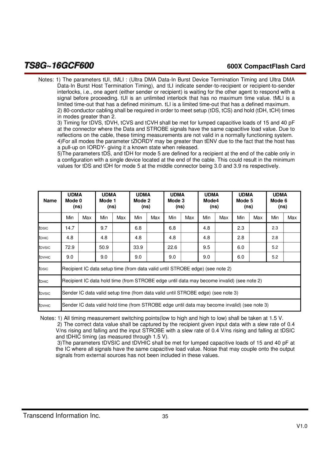
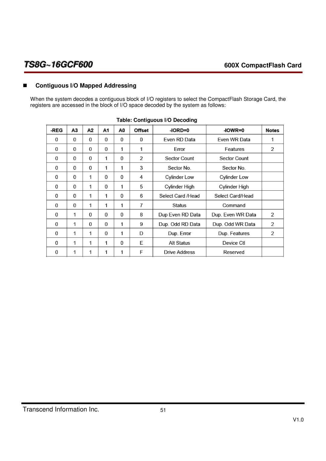
| UDMA Mode | UDMA | UDMA | UDMA | UDMA | UDMA |
| UDMA | Measure |
| ||||||||
|
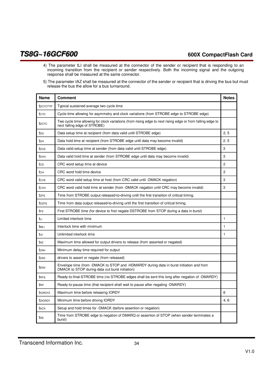
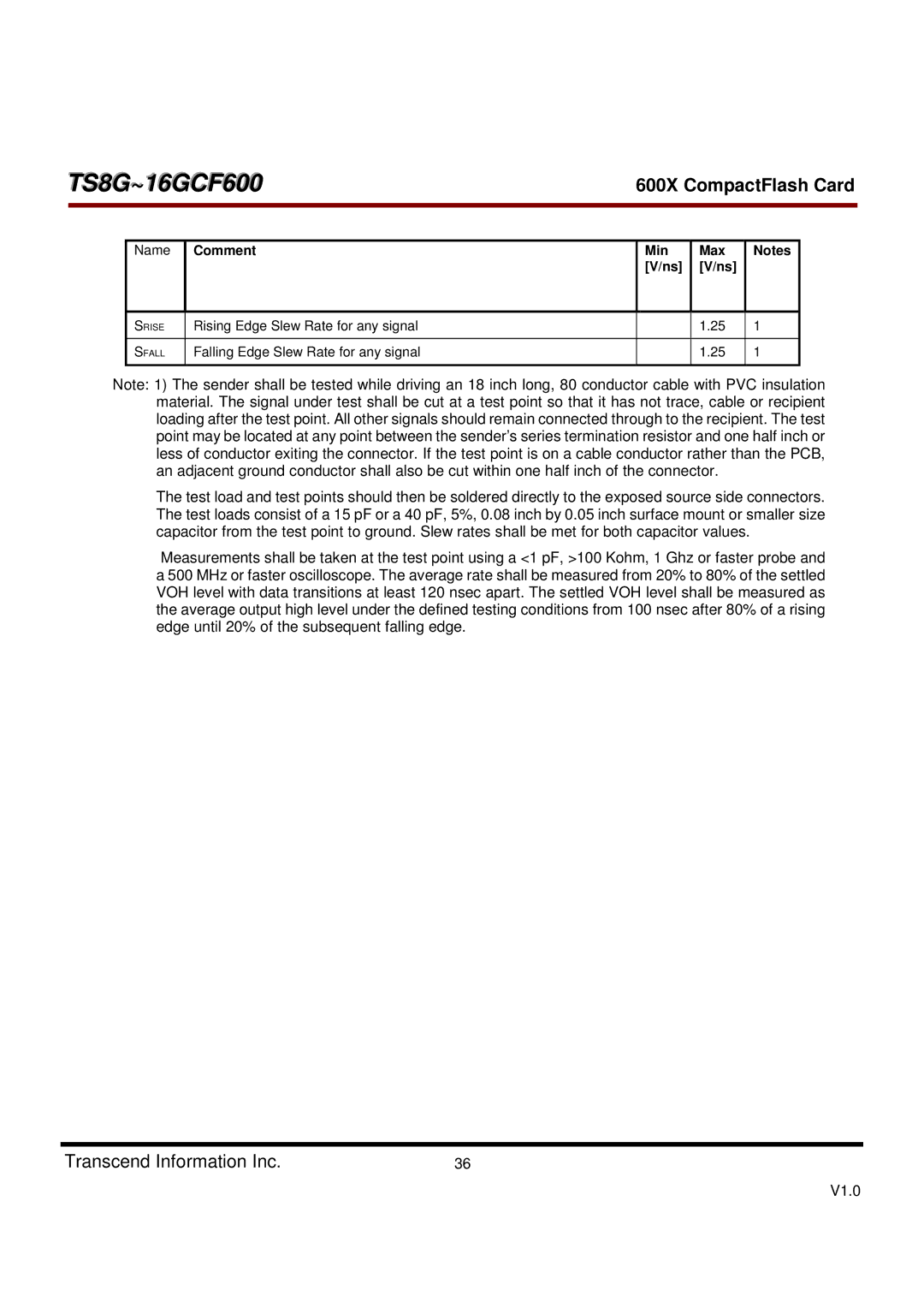
| Name |
| location (see |
| |||||||||||||||
|
|
| 0 | Mode 1 | Mode 2 | Mode 3 | Mode 4 | Mode 5 |
| Mode 6 |
| |||||||||
|
|
|
|
| Note 2) |
| ||||||||||||||
|
|
|
|
|
|
|
|
|
|
|
|
|
|
|
|
|
|
|
| |
|
|
| Min |
| Max | Min | Max | Min | Max | Min | Max | Min | Max | Min | Max |
| Min | Max |
|
|
|
|
|
|
|
|
|
|
|
|
|
|
|
|
|
|
|
|
|
|
|
|
| t2CYCTYP | 240 |
|
| 160 |
| 120 |
| 90 |
| 60 |
| 40 |
|
| 30 |
| Sender |
|
|
|
|
|
|
|
|
|
|
|
|
|
|
|
|
|
|
|
|
|
|
|
| tCYC | 112 |
|
| 73 |
| 54 |
| 39 |
| 25 |
| 16.8 |
|
| 13.0 |
| Note 3 |
|
|
|
|
|
|
|
|
|
|
|
|
|
|
|
|
|
|
|
|
|
|
|
| t2CYC | 230 |
|
| 153 |
| 115 |
| 86 |
| 57 |
| 38 |
|
| 29 |
| Sender |
|
|
|
|
|
|
|
|
|
|
|
|
|
|
|
|
|
|
|
|
|
|
|
| tDS | 15.0 |
|
| 10.0 |
| 7.0 |
| 7.0 |
| 5.0 |
| 4.0 |
|
| 2.6 |
| Recipient |
|
|
|
|
|
|
|
|
|
|
|
|
|
|
|
|
|
|
|
|
|
|
|
| tDH | 5.0 |
|
| 5.0 |
| 5.0 |
| 5.0 |
| 5.0 |
| 4.6 |
|
| 3.5 |
| Recipient |
|
|
|
|
|
|
|
|
|
|
|
|
|
|
|
|
|
|
|
|
|
|
|
| tDVS | 70.0 |
|
| 48.0 |
| 31.0 |
| 20.0 |
| 6.7 |
| 4.8 |
|
| 4.0 |
| Sender |
|
|
|
|
|
|
|
|
|
|
|
|
|
|
|
|
|
|
|
|
|
|
|
| tDVH | 6.2 |
|
| 6.2 |
| 6.2 |
| 6.2 |
| 6.2 |
| 4.8 |
|
| 4.0 |
| Sender |
|
|
|
|
|
|
|
|
|
|
|
|
|
|
|
|
|
|
|
|
|
|
|
| tCS | 15.0 |
|
| 10.0 |
| 7.0 |
| 7.0 |
| 5.0 |
| 5.0 |
|
| 5.0 |
| Device |
|
|
|
|
|
|
|
|
|
|
|
|
|
|
|
|
|
|
|
|
|
|
|
| tCH | 5.0 |
|
| 5.0 |
| 5.0 |
| 5.0 |
| 5.0 |
| 5.0 |
|
| 5.0 |
| Device |
|
|
|
|
|
|
|
|
|
|
|
|
|
|
|
|
|
|
|
|
|
|
|
| tCVS | 70.0 |
|
| 48.0 |
| 31.0 |
| 20.0 |
| 6.7 |
| 10.0 |
|
| 10.0 |
| Host |
|
|
|
|
|
|
|
|
|
|
|
|
|
|
|
|
|
|
|
|
|
|
|
| tCVH | 6.2 |
|
| 6.2 |
| 6.2 |
| 6.2 |
| 6.2 |
| 10.0 |
|
| 10.0 |
| Host |
|
|
|
|
|
|
|
|
|
|
|
|
|
|
|
|
|
|
|
|
|
|
|
| tZFS | 0 |
|
| 0 |
| 0 |
| 0 |
| 0 |
| 35 |
|
| 25 |
| Device |
|
|
|
|
|
|
|
|
|
|
|
|
|
|
|
|
|
|
|
|
|
|
|
| tDZFS | 70.0 |
|
| 48.0 |
| 31.0 |
| 20.0 |
| 6.7 |
| 25 |
|
| 17.5 |
| Sender |
|
|
|
|
|
|
|
|
|
|
|
|
|
|
|
|
|
|
|
|
|
|
|
| tFS |
|
| 230 |
| 200 |
| 170 |
| 130 |
| 120 |
| 90 |
|
| 80 | Device |
|
|
|
|
|
|
|
|
|
|
|
|
|
|
|
|
|
|
|
|
|
|
|
| tLI | 0 |
| 150 | 0 | 150 | 0 | 150 | 0 | 100 | 0 | 100 | 0 | 75 |
| 0 | 60 | Note 4 |
|
|
|
|
|
|
|
|
|
|
|
|
|
|
|
|
|
|
|
|
|
|
|
| tMLI | 20 |
|
| 20 |
| 20 |
| 20 |
| 20 |
| 20 |
|
| 20 |
| Host |
|
|
|
|
|
|
|
|
|
|
|
|
|
|
|
|
|
|
|
|
|
|
|
| tUI | 0 |
|
| 0 |
| 0 |
| 0 |
| 0 |
| 0 |
|
| 0 |
| Host |
|
|
|
|
|
|
|
|
|
|
|
|
|
|
|
|
|
|
|
|
|
|
|
| tAZ |
|
| 10 |
| 10 |
| 10 |
| 10 |
| 10 |
| 10 |
|
| 10 | Note 5 |
|
|
|
|
|
|
|
|
|
|
|
|
|
|
|
|
|
|
|
|
|
|
|
| tZAH | 20 |
|
| 20 |
| 20 |
| 20 |
| 20 |
| 20 |
|
| 20 |
| Host |
|
|
|
|
|
|
|
|
|
|
|
|
|
|
|
|
|
|
|
|
|
|
|
| tZAD | 0 |
|
| 0 |
| 0 |
| 0 |
| 0 |
| 0 |
|
| 0 |
| Device |
|
|
|
|
|
|
|
|
|
|
|
|
|
|
|
|
|
|
|
|
|
|
|
| tENV | 20 |
| 70 | 20 | 70 | 20 | 70 | 20 | 55 | 20 | 55 | 20 | 50 |
| 20 | 50 | Host |
|
|
|
|
|
|
|
|
|
|
|
|
|
|
|
|
|
|
|
|
|
|
|
| tRFS |
|
| 75 |
| 70 |
| 60 |
| 60 |
| 60 |
| 50 |
|
| 50 | Sender |
|
|
|
|
|
|
|
|
|
|
|
|
|
|
|
|
|
|
|
|
|
|
|
| tRP | 160 |
|
| 125 |
| 100 |
| 100 |
| 100 |
| 85 |
|
| 85 |
| Recipient |
|
|
|
|
|
|
|
|
|
|
|
|
|
|
|
|
|
|
|
|
|
|
|
| tIORDYZ |
|
| 20 |
| 20 |
| 20 |
| 20 |
| 20 |
| 20 |
|
| 20 | Device |
|
|
|
|
|
|
|
|
|
|
|
|
|
|
|
|
|
|
|
|
|
|
|
| tZIORDY | 0 |
|
| 0 |
| 0 |
| 0 |
| 0 |
| 0 |
|
| 0 |
| Device |
|
|
|
|
|
|
|
|
|
|
|
|
|
|
|
|
|
|
|
|
|
|
|
| tACK | 20 |
|
| 20 |
| 20 |
| 20 |
| 20 |
| 20 |
|
| 20 |
| Host |
|
|
|
|
|
|
|
|
|
|
|
|
|
|
|
|
|
|
|
|
|
|
|
| tSS | 50 |
|
| 50 |
| 50 |
| 50 |
| 50 |
| 50 |
|
| 50 |
| Sender |
|
|
|
|
|
|
|
|
|
|
|
|
|
|
|
|
|
|
|
|
|
|
Notes:
1)All timing measurement switching points (low to high and high to low) shall be taken at 1.5 V.
2)All signal transitions for a timing parameter shall be measured at the connector specified in the measurement location column. For example, in the case of tRFS, both STROBE and
3)The parameter tCYC shall be measured at the recipient’s connector farthest from the sender.
Transcend Information Inc. | 33 |
V1.0