Innovating the HPWay
Agilent Technologies
Copyright@ HEWLETT-PACKARD Company
Multifunction Synthesizer
Regulatory Information
Safety Considerations
Safety Considerationsfor this Instrument
Product Markings
Contents
Reu.200CT88
Service cont’d Section
Introductionto this Section
Replaceable Parts List
Reference Designationsand Abbreviations Used in this Manual
How to Order
Replaceable Parts List Updating Manual Updates
Nable 6-1.Reference Designations
Access
Abbreviations 1
ALC
Abbreviations 2
Rev.01JUL91
Replaceable Parts
Description
Number Code
HPPart Description Number Mfr- Mfr. Part Number Code
Fible 6-3.Replaceable Parts
CAPACITOR-FXD22PF +-5% Poovdc CER 0+-30 Not Assigned
Designation Number
Reference HP Part Description
Mfr
Reference HP Part Description Designation Number
Rev.1 7MAY88
Me 6-3. Replaceable Parts
Reference HP Part Designation Number
Not Assigned Connector Spin M Post Type
DIODE-SWITCHING 80V 200MA 2NS DO45
CONNECTOR-RFSMC M PC 5 W H M
CONNECTOR-RF SMC M PC W H M
Reference
Mfr
HP Part Description
Cable 6-3.Replaceable Parts
RESISTOR-TRMR 1K 10% C TOP-ADJ 17-TRN
RESISTOR-TRMR20K 10% C TOP-ADJ 17-TRN
0698-3430
Mfr. Part Number
Description Mfr
Rev.17MAY88
IC OP AMP Prcn 8-DIP-C PKG
Transistor Array 16-PIN Plstc DIP
IC Instm Ampl CUR 10-DIP-P PKG
IC OP AMP LOW-BIAS-H-IMPD 8-DIP4 PKG
HPPart Description
Nble 6-3. Replaceable Parts
L e 6-3. Replaceable Parts
A10
Ble 6-3.Replaceable Parts
Miscellaneous Parts
HPPart
Designation Number Code
Reference HPPart Description Mfr
Rnftsund Plstem DOME-HD .125DIA
Deck Assy
RIVET-BUND PL-STEM DOME-HD .125DIA
RIVET-BUND Plstem Domehd .125DIA
Not Separaretlyreplaceable
PANEL, Front AY
Keypad Punched
Shield Display
QW. Description
Reference HPPart Designation Number
Qty.Description
Designation Code
Mfrm Mfr. Part Number Code
Lbble 6-3. Replaceable Parts
Order by Description
IZZ-9
Main Deck Assembly Top, 2923A and above
Model 8904A
Main Deck Assembly Bottom
Main Deck Assembly Bottom, Option 006 2948A and above
Reu.30NOV89
Front Panel Assembly, 2923A and above
Rent Panel Assembly, Option 006 2948A and above Reu.30NOV89
Rear Panel Assembly
Rear Panel Assembly, Option 005 2948A and above Rev.30N0
Rev.ZSSEP88
Covers, Labels, and ROMs
Output Cables 1
Output Cables, Option 005 29484 and above 2 Rev.30N0V89
Table of Contents
Rev.15DEC89
Option Conversions
Number 2942A and below
Titled Hardware Modifications
Instrument Modifications
Revision 22987A with HP 08904-8701 0 as A2U12
FRONT-TO-REAR-PANELOUTPUT Conversion Description
Modification Procedure
Parts Required
Tools Required
Operation Verification
Fl Channel Config
Description
REAR-TO-FRONT-PANELOUTPUT Conversion
Rev.15DEC89 Rear-to-Front-Panel Output Conversion
Fl Channel Config
Ront Panel Output Hardware
Output Cable Routing ALL Options
Rev.01JUL91 Firmware UpdatesBardware Modifications
Firmware Updates A2U12 and A2U13
Different function
Serial Prefix 2737A and below
Modification for Possible Ground Wire Shock Hazard
Firmware Updates/Hardware Modifications
Parts Location Shown with Power Supply Removed
Firmware Updates/Hardware Modifications
Ground Wire Wrapping
Modification for Output Overvoltage Protection Improvement
Parts List
HPPartNumber ~~ Qty Description
Fixed Resistor, 261 or
Cabinet Parts Color Change
Modification for Potential Power Supply Short
Reu.15DEC89 Firmware UpdatesIHardwareModifications
1. Modificationfor Front Panel Assembly
Removing the Front Panel
Installingthe Front Panel
Dont-Panel Assembly, 2923A and above
Section Service
A3 or A10 Output Assembly Phase Synchronization Option
Before Applying Power
Safety Considerations
HOW the Section is Organized
Iwarning
Schematic Symbology and Schematic Diagram Notes
Service TOOLS, HELPS, and Information
Pin of socket
Schematic Diagram Notes 1
Schematic Diagram Notes 2
Schematic Diagram Notes 3
Digital Symbology Reference Information
Llzble 8-1.Schematic Diagram Notes 4
Combinational Logic Symbols and Functions
Schematic Diagram Notes 5
Schematic Diagram Notes 6
Digital Symbology Reference Information
Only with D-type flip-flops Gate and Dependency-Binary
Schematic Diagram Notes 7
Miscellaneous
Llable 8-1.Schematic Diagram Notes 8of
Schematic Diagram Notes 9
Service
Active Levels
Schematic Diagram Notes 10
Enable
Schematic Diagram Notes 11
What the Multifunction Synthesizer Can Do
Principles of Operation Overall
How Waveforms Are Generated
Channel a
Generating Staircases in the Phase Accumulator
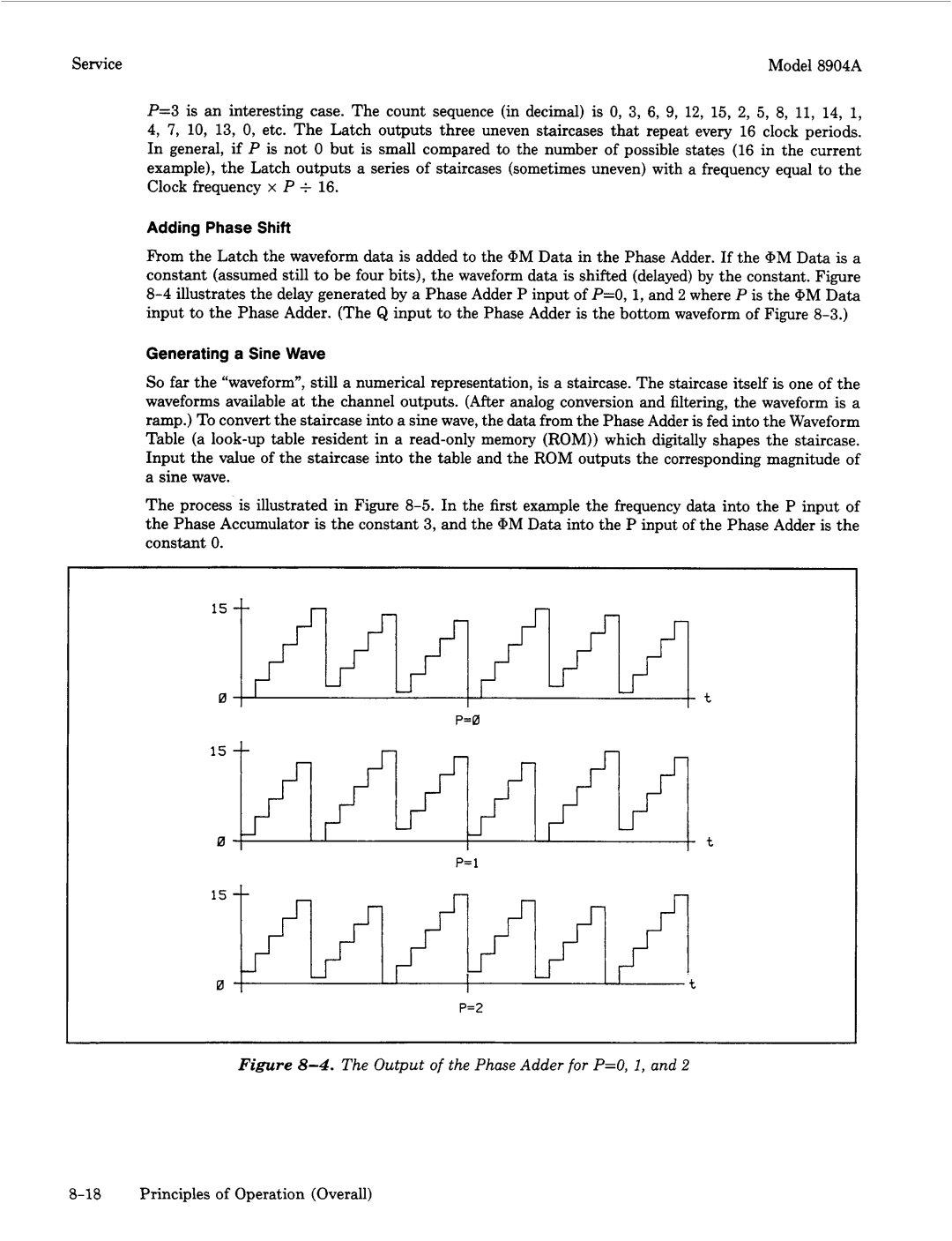
Output of the Phase Adder for P=O, 1,
Further Digital Waveform Processing with Options
Pulse
Phase @PHASE Freouency
Freouency SUM Pulse Level
Interrelationshipof the Circuit Assemblies
Analog Waveform Processing
Reu.15DEC89 Principles of Operation Overall
Synthesizer
PASSY- t
General
A2 Digital Assembly
Digital-to-Analog Converter Service Sheet
A3 Output Assembly Service Sheets 1 through General
Track-and-Hold Circuit Service Sheet
Simplified Diagram of the Sampler Drive
10.Simplified Diagram of the Sampler Amplifier
Audio Amplifier Service Sheet
Low-Pass Filters Service Sheet
Sine X/X CompensationService Sheet
12, and 24 dB Attenuators Service Sheet
Floating Output Amplifier Service Sheet
Floating Amplifier Driver and On/Off Switch Service Sheet
Overvoltage Protectionand Output Circuits Service Sheet
Rev.15DEC89 Troubleshooting General
Troubleshooting General
Procedure
A2 Digital Assembly to A3 or A10 Output Assembly Interface
Equipment
1. How to Access A3 in Instruments Equipped with Option
Serial Prefix
Troubleshooting Digital/Output Interface
Period
Fl Channel Config
Pin Frequency Hz
Fl Channel Config
A3/A10 Connection
Function A3 Key Sequence A10 Key Sequence
IC Pin Level
F3 Memory Map Access
Pin
Clocks A10
J1 and J5
Miscellaneous Control
Fl Keyboard Check
A2 Digital Assembly to A1 Keyboard Assembly Interface
Pin Key Pressed Response lTL
AMPTD, Wave Form
Key Sequence Annunciator Status IC on A2 Pin Level lTL
F3 Memory Map Access
Description
A2 Digital Assembly to A5 Display Assembly Interface
A3 or A10 Output Assembly
Troubleshooting Phase Synchronization
Phase Synchronizationoption
HP 8904A Opts
After keying in 8 7, the display should be
IFirmware Revision 18387A Serial No
HP 8904A Opts 02/01
IFirmware Revision 18387A Serial No
After keying in 4 8, the display should be
Begin again at step
Troubleshooting Memory Backup Battery 48.1
HOW to Replace the Memory Backup Battery
Tools and Supplies
Parts
Troubleshooting Memory Backup Battery
48.3
Rev.15DEC89 Troubleshooting Memory Backup Battery
Page
N a
12.4. Line Voltage Wiring Harness
R300
A3 Component Coordinates 1
L0nA Current Source
Ipower Supply Conditioners
Comp
A3 Component Coordinates 2
Ss2
On the A3 schematic
Rev.28MAR89
31901 N3AILlO ONV
I813IldIll3 JJOlfl3 dWHS
15.Service Sheet Information Component Locator
Rev.28MAR89 54.1
Changes
Ampto Instrument Settings Measure
Aooitions I T I a L Instrument Settings
Coup OUT
K2A
Component Coordinates 1
+ a
56.1
Ss4
Ss4
A6 Schematic and Component locator
Ss5
0 A3/A10
Output Assembly