Chapter 3 | Hardware |
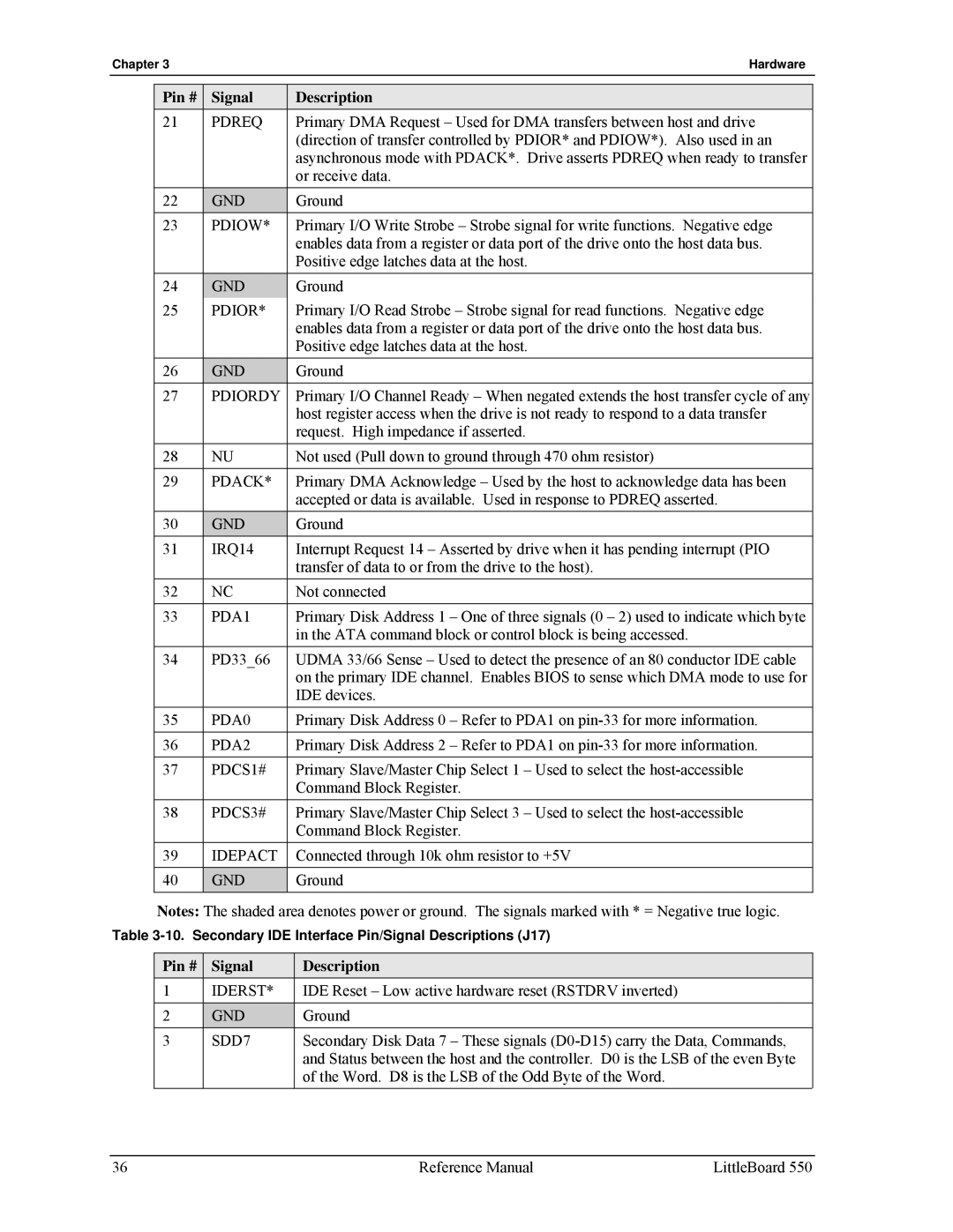
Pin # | Signal | Description |
21 | PDREQ | Primary DMA Request – Used for DMA transfers between host and drive |
|
| (direction of transfer controlled by PDIOR* and PDIOW*). Also used in an |
|
| asynchronous mode with PDACK*. Drive asserts PDREQ when ready to transfer |
|
| or receive data. |
22 | GND | Ground |
23 | PDIOW* | Primary I/O Write Strobe – Strobe signal for write functions. Negative edge |
|
| enables data from a register or data port of the drive onto the host data bus. |
|
| Positive edge latches data at the host. |
24 | GND | Ground |
25 | PDIOR* | Primary I/O Read Strobe – Strobe signal for read functions. Negative edge |
|
| enables data from a register or data port of the drive onto the host data bus. |
|
| Positive edge latches data at the host. |
26 | GND | Ground |
27 | PDIORDY | Primary I/O Channel Ready – When negated extends the host transfer cycle of any |
|
| host register access when the drive is not ready to respond to a data transfer |
|
| request. High impedance if asserted. |
28 | NU | Not used (Pull down to ground through 470 ohm resistor) |
29 | PDACK* | Primary DMA Acknowledge – Used by the host to acknowledge data has been |
|
| accepted or data is available. Used in response to PDREQ asserted. |
30 | GND | Ground |
31 | IRQ14 | Interrupt Request 14 – Asserted by drive when it has pending interrupt (PIO |
|
| transfer of data to or from the drive to the host). |
32 | NC | Not connected |
33 | PDA1 | Primary Disk Address 1 – One of three signals (0 – 2) used to indicate which byte |
|
| in the ATA command block or control block is being accessed. |
34 | PD33_66 | UDMA 33/66 Sense – Used to detect the presence of an 80 conductor IDE cable |
|
| on the primary IDE channel. Enables BIOS to sense which DMA mode to use for |
|
| IDE devices. |
35 | PDA0 | Primary Disk Address 0 – Refer to PDA1 on |
|
|
|
36 | PDA2 | Primary Disk Address 2 – Refer to PDA1 on |
|
|
|
37 | PDCS1# | Primary Slave/Master Chip Select 1 – Used to select the |
|
| Command Block Register. |
38 | PDCS3# | Primary Slave/Master Chip Select 3 – Used to select the |
|
| Command Block Register. |
39 | IDEPACT | Connected through 10k ohm resistor to +5V |
|
|
|
40 | GND | Ground |
Notes: The shaded area denotes power or ground. The signals marked with * = Negative true logic.
Table
Pin # | Signal | Description |
1 | IDERST* | IDE Reset – Low active hardware reset (RSTDRV inverted) |
2 | GND | Ground |
3 | SDD7 | Secondary Disk Data 7 – These signals |
|
| and Status between the host and the controller. D0 is the LSB of the even Byte |
|
| of the Word. D8 is the LSB of the Odd Byte of the Word. |
36 | Reference Manual | LittleBoard 550 |