Chapter 3 | Hardware |
PC/104 Interface (J1A,B,C,D)
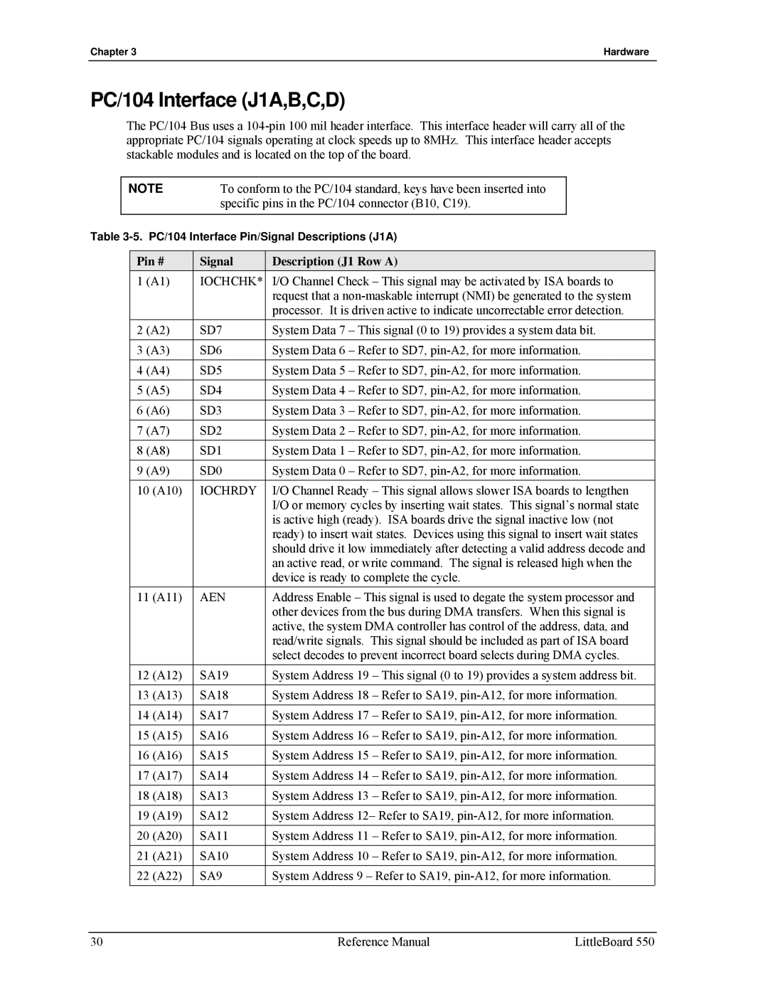
The PC/104 Bus uses a
| NOTE | To conform to the PC/104 standard, keys have been inserted into |
| ||
|
|
| specific pins in the PC/104 connector (B10, C19). |
| |
|
|
|
|
|
|
Table | |||||
|
|
|
|
| |
|
| Pin # | Signal | Description (J1 Row A) | |
|
| 1 (A1) | IOCHCHK* | I/O Channel Check – This signal may be activated by ISA boards to | |
|
|
|
| request that a | |
|
|
|
| processor. It is driven active to indicate uncorrectable error detection. | |
|
| 2 (A2) | SD7 | System Data 7 – This signal (0 to 19) provides a system data bit. | |
|
|
|
|
| |
|
| 3 (A3) | SD6 | System Data 6 – Refer to SD7, | |
|
|
|
|
| |
|
| 4 (A4) | SD5 | System Data 5 – Refer to SD7, | |
|
| 5 (A5) | SD4 | System Data 4 – Refer to SD7, | |
|
|
|
|
| |
|
| 6 (A6) | SD3 | System Data 3 – Refer to SD7, | |
|
|
|
|
| |
|
| 7 (A7) | SD2 | System Data 2 – Refer to SD7, | |
|
| 8 (A8) | SD1 | System Data 1 – Refer to SD7, | |
|
|
|
|
| |
|
| 9 (A9) | SD0 | System Data 0 – Refer to SD7, | |
|
|
|
|
| |
|
| 10 (A10) | IOCHRDY | I/O Channel Ready – This signal allows slower ISA boards to lengthen | |
|
|
|
| I/O or memory cycles by inserting wait states. This signal’s normal state | |
|
|
|
| is active high (ready). ISA boards drive the signal inactive low (not | |
|
|
|
| ready) to insert wait states. Devices using this signal to insert wait states | |
|
|
|
| should drive it low immediately after detecting a valid address decode and | |
|
|
|
| an active read, or write command. The signal is released high when the | |
|
|
|
| device is ready to complete the cycle. | |
|
| 11 (A11) | AEN | Address Enable – This signal is used to degate the system processor and | |
|
|
|
| other devices from the bus during DMA transfers. When this signal is | |
|
|
|
| active, the system DMA controller has control of the address, data, and | |
|
|
|
| read/write signals. This signal should be included as part of ISA board | |
|
|
|
| select decodes to prevent incorrect board selects during DMA cycles. | |
|
| 12 (A12) | SA19 | System Address 19 – This signal (0 to 19) provides a system address bit. | |
|
| 13 (A13) | SA18 | System Address 18 – Refer to SA19, | |
|
|
|
|
| |
|
| 14 (A14) | SA17 | System Address 17 – Refer to SA19, | |
|
|
|
|
| |
|
| 15 (A15) | SA16 | System Address 16 – Refer to SA19, | |
|
|
|
|
| |
|
| 16 (A16) | SA15 | System Address 15 – Refer to SA19, | |
|
|
|
|
| |
|
| 17 (A17) | SA14 | System Address 14 – Refer to SA19, | |
|
|
|
|
| |
|
| 18 (A18) | SA13 | System Address 13 – Refer to SA19, | |
|
|
|
|
| |
|
| 19 (A19) | SA12 | System Address 12– Refer to SA19, | |
|
| 20 (A20) | SA11 | System Address 11 – Refer to SA19, | |
|
|
|
|
| |
|
| 21 (A21) | SA10 | System Address 10 – Refer to SA19, | |
|
|
|
|
| |
|
| 22 (A22) | SA9 | System Address 9 – Refer to SA19, | |
30 | Reference Manual | LittleBoard 550 |