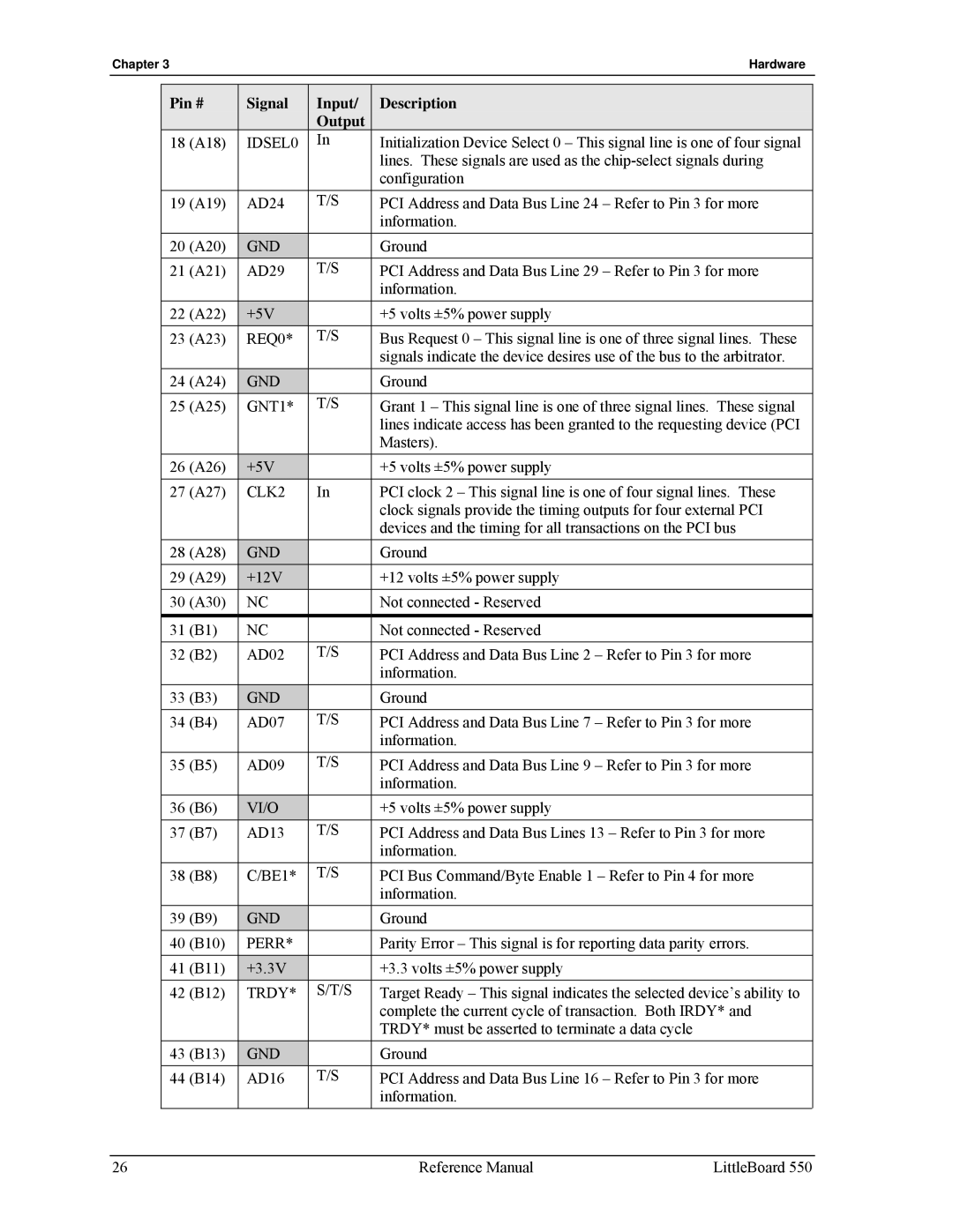
Chapter 3 | Hardware |
Pin # | Signal | Input/ | Description | |
|
|
| Output |
|
18 | (A18) | IDSEL0 | In | Initialization Device Select 0 – This signal line is one of four signal |
|
|
|
| lines. These signals are used as the |
|
|
|
| configuration |
19 | (A19) | AD24 | T/S | PCI Address and Data Bus Line 24 – Refer to Pin 3 for more |
|
|
|
| information. |
20 | (A20) | GND |
| Ground |
21 | (A21) | AD29 | T/S | PCI Address and Data Bus Line 29 – Refer to Pin 3 for more |
|
|
|
| information. |
22 | (A22) | +5V |
| +5 volts ±5% power supply |
23 | (A23) | REQ0* | T/S | Bus Request 0 – This signal line is one of three signal lines. These |
|
|
|
| signals indicate the device desires use of the bus to the arbitrator. |
24 | (A24) | GND |
| Ground |
25 | (A25) | GNT1* | T/S | Grant 1 – This signal line is one of three signal lines. These signal |
|
|
|
| lines indicate access has been granted to the requesting device (PCI |
|
|
|
| Masters). |
26 | (A26) | +5V |
| +5 volts ±5% power supply |
27 | (A27) | CLK2 | In | PCI clock 2 – This signal line is one of four signal lines. These |
|
|
|
| clock signals provide the timing outputs for four external PCI |
|
|
|
| devices and the timing for all transactions on the PCI bus |
28 | (A28) | GND |
| Ground |
29 | (A29) | +12V |
| +12 volts ±5% power supply |
30 | (A30) | NC |
| Not connected - Reserved |
|
|
|
|
|
31 | (B1) | NC |
| Not connected - Reserved |
|
|
|
|
|
32 | (B2) | AD02 | T/S | PCI Address and Data Bus Line 2 – Refer to Pin 3 for more |
|
|
|
| information. |
33 | (B3) | GND |
| Ground |
34 | (B4) | AD07 | T/S | PCI Address and Data Bus Line 7 – Refer to Pin 3 for more |
|
|
|
| information. |
35 | (B5) | AD09 | T/S | PCI Address and Data Bus Line 9 – Refer to Pin 3 for more |
|
|
|
| information. |
36 | (B6) | VI/O |
| +5 volts ±5% power supply |
37 | (B7) | AD13 | T/S | PCI Address and Data Bus Lines 13 – Refer to Pin 3 for more |
|
|
|
| information. |
38 | (B8) | C/BE1* | T/S | PCI Bus Command/Byte Enable 1 – Refer to Pin 4 for more |
|
|
|
| information. |
39 | (B9) | GND |
| Ground |
40 | (B10) | PERR* |
| Parity Error – This signal is for reporting data parity errors. |
|
|
|
|
|
41 | (B11) | +3.3V |
| +3.3 volts ±5% power supply |
42 | (B12) | TRDY* | S/T/S | Target Ready – This signal indicates the selected device’s ability to |
|
|
|
| complete the current cycle of transaction. Both IRDY* and |
|
|
|
| TRDY* must be asserted to terminate a data cycle |
43 | (B13) | GND |
| Ground |
44 | (B14) | AD16 | T/S | PCI Address and Data Bus Line 16 – Refer to Pin 3 for more |
|
|
|
| information. |
26 | Reference Manual | LittleBoard 550 |