AD9912
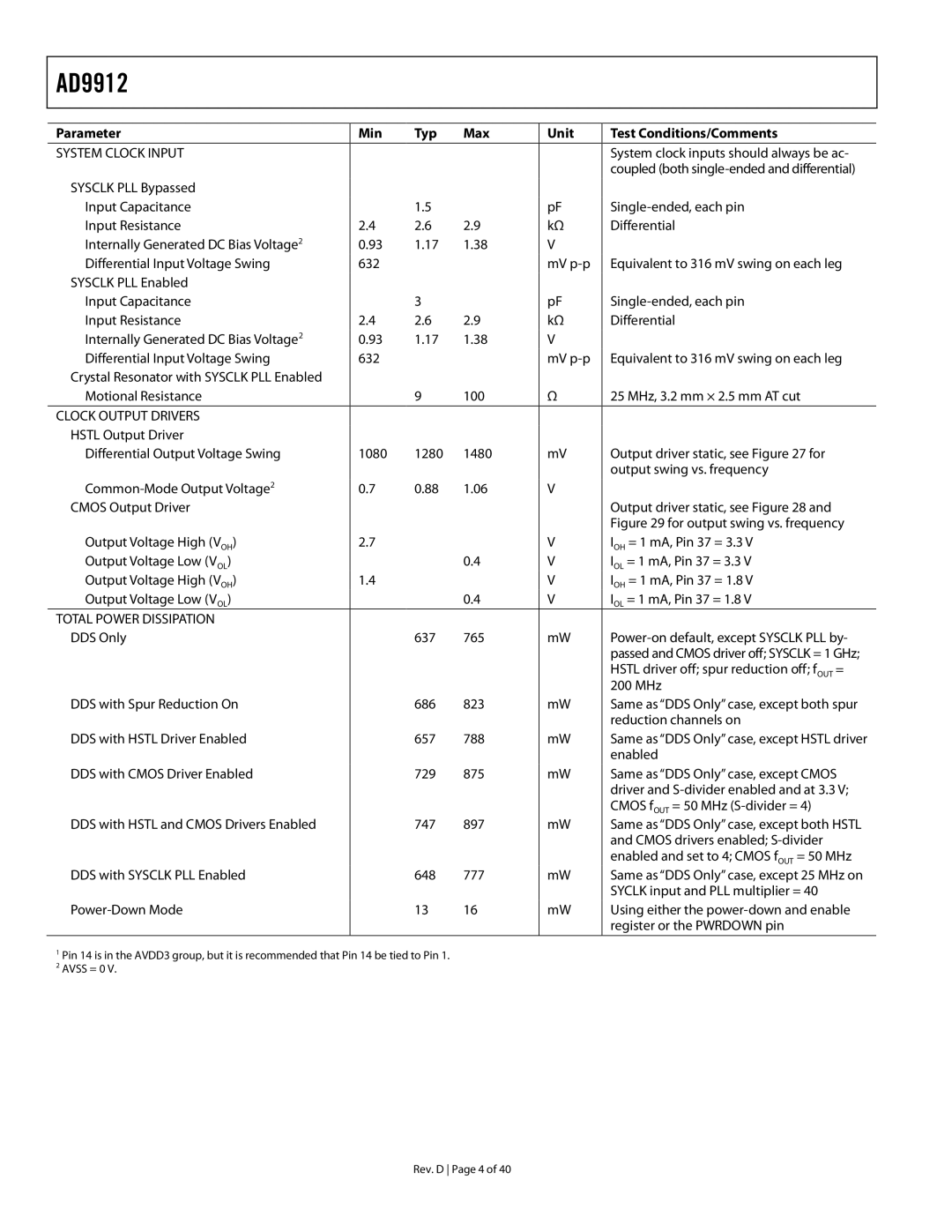
Parameter | Min | Typ | Max | Unit | Test Conditions/Comments |
SYSTEM CLOCK INPUT |
|
|
|
| System clock inputs should always be ac- |
|
|
|
|
| coupled (both |
SYSCLK PLL Bypassed |
|
|
|
|
|
Input Capacitance |
| 1.5 |
| pF | |
Input Resistance | 2.4 | 2.6 | 2.9 | kΩ | Differential |
Internally Generated DC Bias Voltage2 | 0.93 | 1.17 | 1.38 | V |
|
Differential Input Voltage Swing | 632 |
|
| mV | Equivalent to 316 mV swing on each leg |
SYSCLK PLL Enabled |
|
|
|
|
|
Input Capacitance |
| 3 |
| pF | |
Input Resistance | 2.4 | 2.6 | 2.9 | kΩ | Differential |
Internally Generated DC Bias Voltage2 | 0.93 | 1.17 | 1.38 | V |
|
Differential Input Voltage Swing | 632 |
|
| mV | Equivalent to 316 mV swing on each leg |
Crystal Resonator with SYSCLK PLL Enabled |
|
|
|
|
|
Motional Resistance |
| 9 | 100 | Ω | 25 MHz, 3.2 mm × 2.5 mm AT cut |
|
|
|
|
|
|
CLOCK OUTPUT DRIVERS |
|
|
|
|
|
HSTL Output Driver |
|
|
|
|
|
Differential Output Voltage Swing | 1080 | 1280 | 1480 | mV | Output driver static, see Figure 27 for |
|
|
|
|
| output swing vs. frequency |
0.7 | 0.88 | 1.06 | V |
| |
CMOS Output Driver |
|
|
|
| Output driver static, see Figure 28 and |
|
|
|
|
| Figure 29 for output swing vs. frequency |
Output Voltage High (VOH) | 2.7 |
|
| V | IOH = 1 mA, Pin 37 = 3.3 V |
Output Voltage Low (VOL) |
|
| 0.4 | V | IOL = 1 mA, Pin 37 = 3.3 V |
Output Voltage High (VOH) | 1.4 |
|
| V | IOH = 1 mA, Pin 37 = 1.8 V |
Output Voltage Low (VOL) |
|
| 0.4 | V | IOL = 1 mA, Pin 37 = 1.8 V |
TOTAL POWER DISSIPATION |
|
|
|
|
|
DDS Only |
| 637 | 765 | mW | |
|
|
|
|
| passed and CMOS driver off; SYSCLK = 1 GHz; |
|
|
|
|
| HSTL driver off; spur reduction off; fOUT = |
|
|
|
|
| 200 MHz |
DDS with Spur Reduction On |
| 686 | 823 | mW | Same as “DDS Only” case, except both spur |
|
|
|
|
| reduction channels on |
DDS with HSTL Driver Enabled |
| 657 | 788 | mW | Same as “DDS Only” case, except HSTL driver |
|
|
|
|
| enabled |
DDS with CMOS Driver Enabled |
| 729 | 875 | mW | Same as “DDS Only” case, except CMOS |
|
|
|
|
| driver and |
|
|
|
|
| CMOS fOUT = 50 MHz |
DDS with HSTL and CMOS Drivers Enabled |
| 747 | 897 | mW | Same as “DDS Only” case, except both HSTL |
|
|
|
|
| and CMOS drivers enabled; |
|
|
|
|
| enabled and set to 4; CMOS fOUT = 50 MHz |
DDS with SYSCLK PLL Enabled |
| 648 | 777 | mW | Same as “DDS Only” case, except 25 MHz on |
|
|
|
|
| SYCLK input and PLL multiplier = 40 |
| 13 | 16 | mW | Using either the | |
|
|
|
|
| register or the PWRDOWN pin |
|
|
|
|
|
|
1Pin 14 is in the AVDD3 group, but it is recommended that Pin 14 be tied to Pin 1.
2AVSS = 0 V.
Rev. D Page 4 of 40
