AD9912
AC SPECIFICATIONS
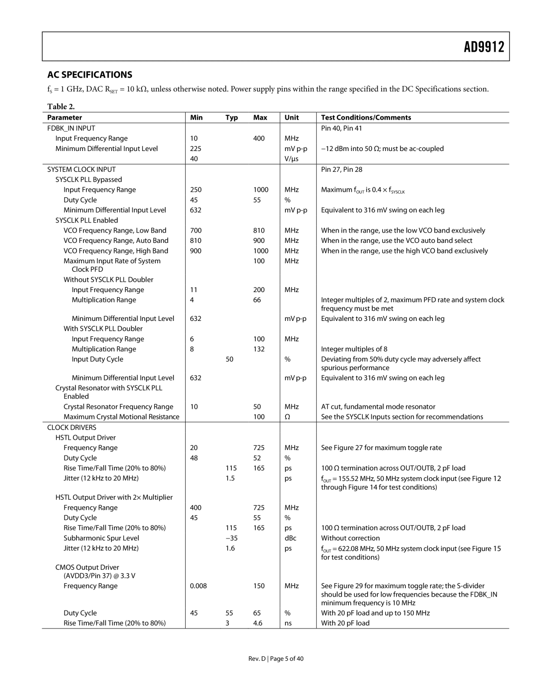
fS = 1 GHz, DAC RSET = 10 kΩ, unless otherwise noted. Power supply pins within the range specified in the DC Specifications section.
Table 2.
Parameter | Min | Typ | Max | Unit | Test Conditions/Comments |
|
|
|
|
|
|
FDBK_IN INPUT |
|
|
|
| Pin 40, Pin 41 |
Input Frequency Range | 10 |
| 400 | MHz |
|
Minimum Differential Input Level | 225 |
|
| mV | −12 dBm into 50 Ω; must be |
| 40 |
|
| V/μs |
|
SYSTEM CLOCK INPUT |
|
|
|
| Pin 27, Pin 28 |
SYSCLK PLL Bypassed |
|
|
|
|
|
Input Frequency Range | 250 |
| 1000 | MHz | Maximum fOUT is 0.4 × fSYSCLK |
Duty Cycle | 45 |
| 55 | % |
|
Minimum Differential Input Level | 632 |
|
| mV | Equivalent to 316 mV swing on each leg |
SYSCLK PLL Enabled |
|
|
|
|
|
VCO Frequency Range, Low Band | 700 |
| 810 | MHz | When in the range, use the low VCO band exclusively |
VCO Frequency Range, Auto Band | 810 |
| 900 | MHz | When in the range, use the VCO auto band select |
VCO Frequency Range, High Band | 900 |
| 1000 | MHz | When in the range, use the high VCO band exclusively |
Maximum Input Rate of System |
|
| 100 | MHz |
|
Clock PFD |
|
|
|
|
|
Without SYSCLK PLL Doubler |
|
|
|
|
|
Input Frequency Range | 11 |
| 200 | MHz |
|
Multiplication Range | 4 |
| 66 |
| Integer multiples of 2, maximum PFD rate and system clock |
|
|
|
|
| frequency must be met |
Minimum Differential Input Level | 632 |
|
| mV | Equivalent to 316 mV swing on each leg |
With SYSCLK PLL Doubler |
|
|
|
|
|
Input Frequency Range | 6 |
| 100 | MHz |
|
Multiplication Range | 8 |
| 132 |
| Integer multiples of 8 |
Input Duty Cycle |
| 50 |
| % | Deviating from 50% duty cycle may adversely affect |
|
|
|
|
| spurious performance |
Minimum Differential Input Level | 632 |
|
| mV | Equivalent to 316 mV swing on each leg |
Crystal Resonator with SYSCLK PLL |
|
|
|
|
|
Enabled |
|
|
|
|
|
Crystal Resonator Frequency Range | 10 |
| 50 | MHz | AT cut, fundamental mode resonator |
Maximum Crystal Motional Resistance |
|
| 100 | Ω | See the SYSCLK Inputs section for recommendations |
CLOCK DRIVERS |
|
|
|
|
|
HSTL Output Driver |
|
|
|
|
|
Frequency Range | 20 |
| 725 | MHz | See Figure 27 for maximum toggle rate |
Duty Cycle | 48 |
| 52 | % |
|
Rise Time/Fall Time (20% to 80%) |
| 115 | 165 | ps | 100 Ω termination across OUT/OUTB, 2 pF load |
Jitter (12 kHz to 20 MHz) |
| 1.5 |
| ps | fOUT = 155.52 MHz, 50 MHz system clock input (see Figure 12 |
|
|
|
|
| through Figure 14 for test conditions) |
HSTL Output Driver with 2× Multiplier |
|
|
|
|
|
Frequency Range | 400 |
| 725 | MHz |
|
Duty Cycle | 45 |
| 55 | % |
|
Rise Time/Fall Time (20% to 80%) |
| 115 | 165 | ps | 100 Ω termination across OUT/OUTB, 2 pF load |
Subharmonic Spur Level |
| −35 |
| dBc | Without correction |
Jitter (12 kHz to 20 MHz) |
| 1.6 |
| ps | fOUT = 622.08 MHz, 50 MHz system clock input (see Figure 15 |
|
|
|
|
| for test conditions) |
CMOS Output Driver |
|
|
|
|
|
(AVDD3/Pin 37) @ 3.3 V |
|
|
|
|
|
Frequency Range | 0.008 |
| 150 | MHz | See Figure 29 for maximum toggle rate; the |
|
|
|
|
| should be used for low frequencies because the FDBK_IN |
|
|
|
|
| minimum frequency is 10 MHz |
Duty Cycle | 45 | 55 | 65 | % | With 20 pF load and up to 150 MHz |
Rise Time/Fall Time (20% to 80%) |
| 3 | 4.6 | ns | With 20 pF load |
|
|
|
|
|
|
Rev. D Page 5 of 40