AD9912
PIN CONFIGURATION AND FUNCTION DESCRIPTIONS
DVDD_I/O 1 ![]()
![]() DVSS 2
DVSS 2 ![]()
![]() DVDD 3
DVDD 3 ![]()
![]() DVSS 4
DVSS 4 ![]()
![]() DVDD 5
DVDD 5 ![]()
![]() DVSS 6
DVSS 6 ![]()
![]() DVDD 7
DVDD 7 ![]()
![]() DVSS 8
DVSS 8 ![]()
![]()
S1 9 ![]()
S2 10 ![]() AVDD 11
AVDD 11 ![]() NC 12
NC 12 ![]() NC 13
NC 13 ![]() AVDD3 14
AVDD3 14 ![]() NC 15
NC 15 ![]() NC 16
NC 16 ![]()
SCLK SDIO SDO CSB IO UPDATE RESET PWRDOWN DVSS DVSS S4 S3 AVDD AVSS DAC OUTB DAC OUT AVDD3 |
| |||||||||||||||||||
64 63 62 61 60 59 58 57 56 55 54 53 52 51 50 49 |
|
|
| |||||||||||||||||
|
|
|
|
|
|
|
|
|
|
|
|
|
|
|
|
|
|
| 48 DAC_RSET | |
|
|
|
|
|
|
|
|
|
|
|
|
|
|
|
|
|
|
| ||
| PIN 1 |
|
|
| ||||||||||||||||
|
|
| ||||||||||||||||||
| INDICATOR |
|
|
| 47 AVDD3 | |||||||||||||||
|
|
| ||||||||||||||||||
|
|
|
|
|
|
|
|
|
|
|
|
|
|
|
|
|
|
| 46 | AVDD3 |
|
|
|
|
|
|
|
|
|
|
|
|
|
|
|
|
| ||||
|
|
|
|
|
|
|
|
|
|
|
|
|
|
|
|
|
|
| 45 | AVDD |
|
|
|
|
|
|
|
|
|
|
|
|
|
|
|
|
| ||||
|
|
|
|
|
|
|
|
|
|
|
|
|
|
|
|
|
|
| 44 | AVDD |
|
|
|
|
|
|
|
|
|
|
|
|
|
|
|
|
| ||||
|
|
|
|
|
|
|
|
|
|
|
|
|
|
|
|
|
|
| 43 | AVSS |
|
|
|
|
|
|
|
|
|
|
|
|
|
|
|
|
| ||||
|
|
|
|
|
| AD9912 |
|
|
| 42 | AVDD | |||||||||
|
|
|
|
|
|
| ||||||||||||||
|
|
|
|
|
|
|
|
| 41 | FDBK_IN | ||||||||||
|
|
|
|
|
| TOP VIEW |
|
|
| |||||||||||
|
|
|
|
|
|
|
|
| 40 | FDBK_INB | ||||||||||
|
|
|
|
| (Not to Scale) |
|
|
| ||||||||||||
|
|
|
|
|
|
|
| 39 | AVSS | |||||||||||
|
|
|
|
|
|
|
|
|
|
|
|
|
|
|
|
|
|
| ||
|
|
|
|
|
|
|
|
|
|
|
|
|
|
|
|
|
|
| 38 | OUT_CMOS |
|
|
|
|
|
|
|
|
|
|
|
|
|
|
|
|
| ||||
|
|
|
|
|
|
|
|
|
|
|
|
|
|
|
|
|
|
| 37 | AVDD3 |
|
|
|
|
|
|
|
|
|
|
|
|
|
|
|
|
| ||||
|
|
|
|
|
|
|
|
|
|
|
|
|
|
|
|
|
|
| 36 | AVDD |
|
|
|
|
|
|
|
|
|
|
|
|
|
|
|
|
| ||||
|
|
|
|
|
|
|
|
|
|
|
|
|
|
|
|
|
|
| 35 | OUT |
|
|
|
|
|
|
|
|
|
|
|
|
|
|
|
|
| ||||
|
|
|
|
|
|
|
|
|
|
|
|
|
|
|
|
|
|
| 34 | OUTB |
|
|
|
|
|
|
|
|
|
|
|
|
|
|
|
|
| ||||
|
|
|
|
|
|
|
|
|
|
|
|
|
|
|
|
|
|
| 33 | AVSS |
|
|
|
|
|
|
|
|
|
|
|
|
|
|
|
|
| ||||
|
|
|
|
|
|
|
|
|
|
|
|
|
|
|
|
|
|
| ||
|
|
|
|
|
|
|
|
|
|
|
|
|
|
|
|
|
|
| ||
NC 17 NC 18 AVDD 19 NC 20 NC 21 NC 22 AVDD 23 AVDD 24 AVDD 25 AVDD 26 SYSCLK 27 SYSCLKB 28 AVDD 29 AVDD 30 LOOP FILTER 31 | CLKMODESEL 32 |
| ||||||||||||||||||
NOTES
1.NC = NO CONNECT.
2.THE EXPOSED PAD MUST BE CONNECTED TO GROUND FOR PROPER OPERATION.
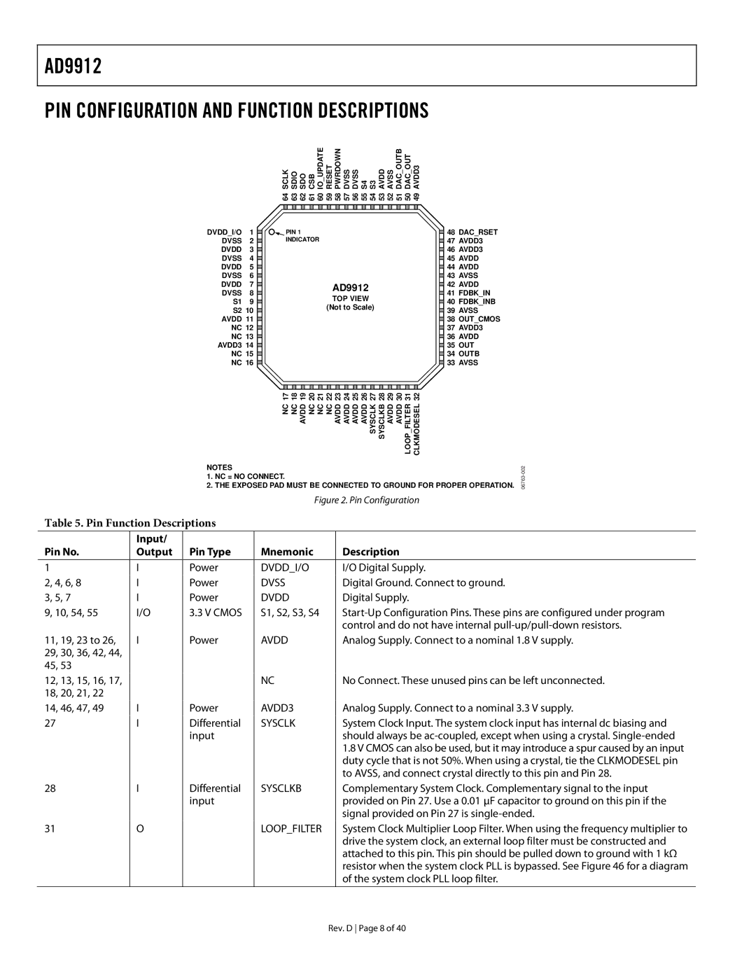
Figure 2. Pin Configuration
Table 5. Pin Function Descriptions
| Input/ |
|
|
|
Pin No. | Output | Pin Type | Mnemonic | Description |
1 | I | Power | DVDD_I/O | I/O Digital Supply. |
2, 4, 6, 8 | I | Power | DVSS | Digital Ground. Connect to ground. |
3, 5, 7 | I | Power | DVDD | Digital Supply. |
9, 10, 54, 55 | I/O | 3.3 V CMOS | S1, S2, S3, S4 | |
|
|
|
| control and do not have internal |
11, 19, 23 to 26, | I | Power | AVDD | Analog Supply. Connect to a nominal 1.8 V supply. |
29, 30, 36, 42, 44, |
|
|
|
|
45, 53 |
|
|
|
|
12, 13, 15, 16, 17, |
|
| NC | No Connect. These unused pins can be left unconnected. |
18, 20, 21, 22 |
|
|
|
|
14, 46, 47, 49 | I | Power | AVDD3 | Analog Supply. Connect to a nominal 3.3 V supply. |
27 | I | Differential | SYSCLK | System Clock Input. The system clock input has internal dc biasing and |
|
| input |
| should always be |
|
|
|
| 1.8 V CMOS can also be used, but it may introduce a spur caused by an input |
|
|
|
| duty cycle that is not 50%. When using a crystal, tie the CLKMODESEL pin |
|
|
|
| to AVSS, and connect crystal directly to this pin and Pin 28. |
28 | I | Differential | SYSCLKB | Complementary System Clock. Complementary signal to the input |
|
| input |
| provided on Pin 27. Use a 0.01 μF capacitor to ground on this pin if the |
|
|
|
| signal provided on Pin 27 is |
31 | O |
| LOOP_FILTER | System Clock Multiplier Loop Filter. When using the frequency multiplier to |
|
|
|
| drive the system clock, an external loop filter must be constructed and |
|
|
|
| attached to this pin. This pin should be pulled down to ground with 1 kΩ |
|
|
|
| resistor when the system clock PLL is bypassed. See Figure 46 for a diagram |
|
|
|
| of the system clock PLL loop filter. |
Rev. D Page 8 of 40