AD9912
SPECIFICATIONS
DC SPECIFICATIONS
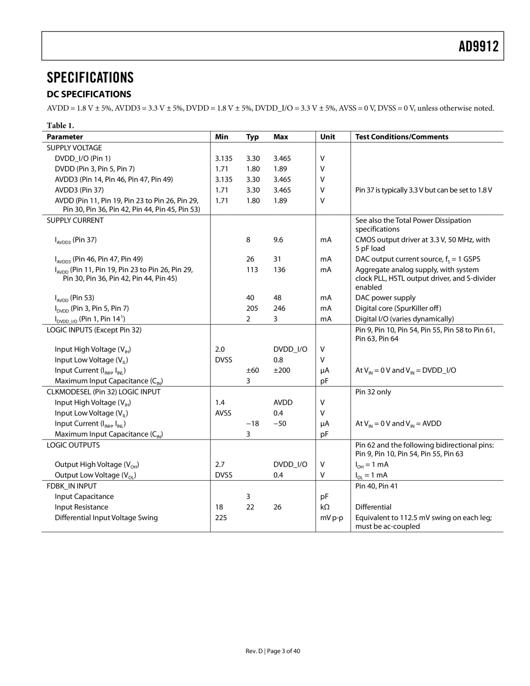
AVDD = 1.8 V ± 5%, AVDD3 = 3.3 V ± 5%, DVDD = 1.8 V ± 5%, DVDD_I/O = 3.3 V ± 5%, AVSS = 0 V, DVSS = 0 V, unless otherwise noted.
Table 1.
Parameter | Min | Typ | Max | Unit | Test Conditions/Comments |
|
|
|
|
|
|
SUPPLY VOLTAGE |
|
|
|
|
|
DVDD_I/O (Pin 1) | 3.135 | 3.30 | 3.465 | V |
|
DVDD (Pin 3, Pin 5, Pin 7) | 1.71 | 1.80 | 1.89 | V |
|
AVDD3 (Pin 14, Pin 46, Pin 47, Pin 49) | 3.135 | 3.30 | 3.465 | V |
|
AVDD3 (Pin 37) | 1.71 | 3.30 | 3.465 | V | Pin 37 is typically 3.3 V but can be set to 1.8 V |
AVDD (Pin 11, Pin 19, Pin 23 to Pin 26, Pin 29, | 1.71 | 1.80 | 1.89 | V |
|
Pin 30, Pin 36, Pin 42, Pin 44, Pin 45, Pin 53) |
|
|
|
|
|
SUPPLY CURRENT |
|
|
|
| See also the Total Power Dissipation |
|
|
|
|
| specifications |
IAVDD3 (Pin 37) |
| 8 | 9.6 | mA | CMOS output driver at 3.3 V, 50 MHz, with |
|
|
|
|
| 5 pF load |
IAVDD3 (Pin 46, Pin 47, Pin 49) |
| 26 | 31 | mA | DAC output current source, fS = 1 GSPS |
IAVDD (Pin 11, Pin 19, Pin 23 to Pin 26, Pin 29, |
| 113 | 136 | mA | Aggregate analog supply, with system |
Pin 30, Pin 36, Pin 42, Pin 44, Pin 45) |
|
|
|
| clock PLL, HSTL output driver, and |
|
|
|
|
| enabled |
IAVDD (Pin 53) |
| 40 | 48 | mA | DAC power supply |
IDVDD (Pin 3, Pin 5, Pin 7) |
| 205 | 246 | mA | Digital core (SpurKiller off) |
IDVDD_I/O (Pin 1, Pin 141) |
| 2 | 3 | mA | Digital I/O (varies dynamically) |
LOGIC INPUTS (Except Pin 32) |
|
|
|
| Pin 9, Pin 10, Pin 54, Pin 55, Pin 58 to Pin 61, |
|
|
|
|
| Pin 63, Pin 64 |
Input High Voltage (VIH) | 2.0 |
| DVDD_I/O | V |
|
Input Low Voltage (VIL) | DVSS |
| 0.8 | V |
|
Input Current (IINH, IINL) |
| ±60 | ±200 | µA | At VIN = 0 V and VIN = DVDD_I/O |
Maximum Input Capacitance (CIN) |
| 3 |
| pF |
|
CLKMODESEL (Pin 32) LOGIC INPUT |
|
|
|
| Pin 32 only |
Input High Voltage (VIH) | 1.4 |
| AVDD | V |
|
Input Low Voltage (VIL) | AVSS |
| 0.4 | V |
|
Input Current (IINH, IINL) |
| −18 | −50 | µA | At VIN = 0 V and VIN = AVDD |
Maximum Input Capacitance (CIN) |
| 3 |
| pF |
|
LOGIC OUTPUTS |
|
|
|
| Pin 62 and the following bidirectional pins: |
|
|
|
|
| Pin 9, Pin 10, Pin 54, Pin 55, Pin 63 |
Output High Voltage (VOH) | 2.7 |
| DVDD_I/O | V | IOH = 1 mA |
Output Low Voltage (VOL) | DVSS |
| 0.4 | V | IOL = 1 mA |
FDBK_IN INPUT |
|
|
|
| Pin 40, Pin 41 |
Input Capacitance |
| 3 |
| pF |
|
Input Resistance | 18 | 22 | 26 | kΩ | Differential |
Differential Input Voltage Swing | 225 |
|
| mV | Equivalent to 112.5 mV swing on each leg; |
|
|
|
|
| must be |
|
|
|
|
|
|
Rev. D Page 3 of 40