QY8-1360-000 specifications
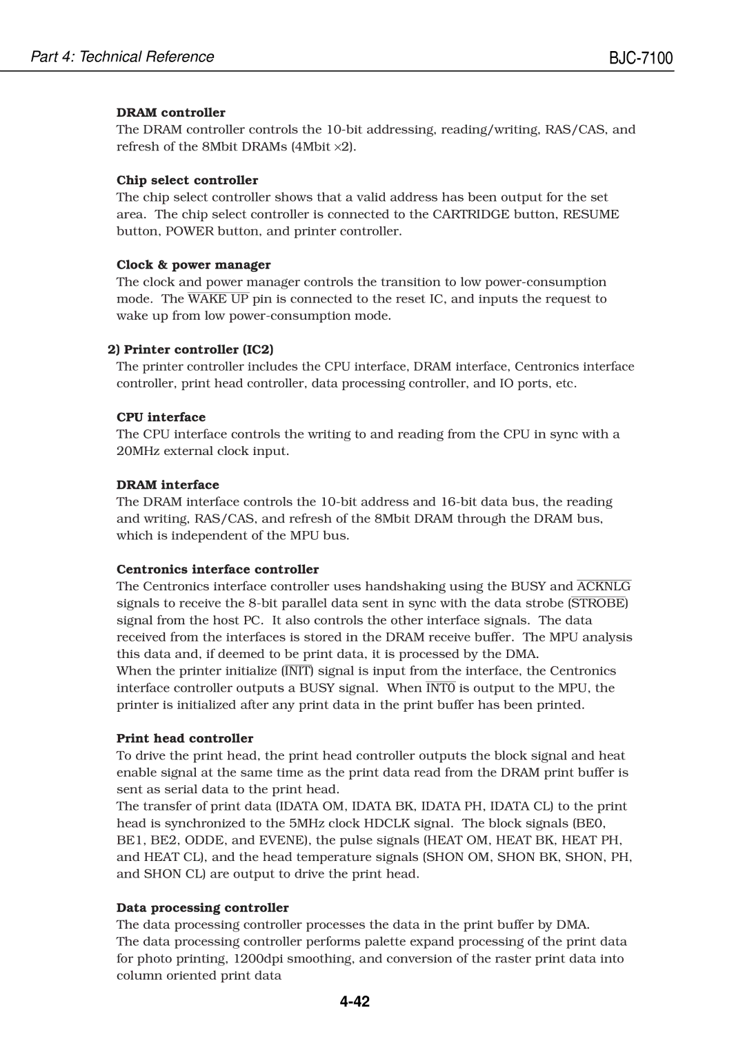
The Canon QY8-1360-000 is a highly regarded print head designed specifically for Canon’s line of professional printers, particularly those used in high-quality photo printing and graphic arts. This component is essential for achieving the vibrant colors and sharp details that are hallmark features of Canon’s imaging technology.One of the main features of the QY8-1360-000 is its precision engineering, which allows for a high level of accuracy in ink application. This print head utilizes a micro-nozzle technology that enhances the distribution of ink onto the paper, minimizing the potential for blurriness or color bleeding. The micro-nozzles work in conjunction with a sophisticated ink delivery system, ensuring that colors are produced as intended by the original digital file.
Another key characteristic of the QY8-1360-000 is its ability to support a wide range of media types, ensuring flexibility for various printing projects. Whether it’s glossy photo paper, fine art paper, or even canvas, this print head can accommodate different textures and finishes, making it ideal for both professional photographers and graphic designers.
Additionally, this print head is designed to achieve high resolution printing, with capabilities that can reach up to 4800 x 1200 dpi. Such high resolution allows for exceptional detail and color accuracy, which is particularly critical when producing photographic prints. The print head can also handle a broad color gamut, facilitating rich and vivid color outputs that elevate the overall quality of printed materials.
Technologically, the QY8-1360-000 incorporates Canon’s FINE (Full-Photolithography Inkjet Nozzle Engineering) technology. This innovative technology allows for the quick heat-up and ejection of ink, ensuring rapid print speeds without compromising quality. By combining speed with precision, it significantly enhances productivity in a professional setting.
In summary, the Canon QY8-1360-000 print head is an essential component for anyone seeking exceptional print quality and versatility in their printing endeavors. With precision engineering, support for multiple media types, high resolution output, and advanced FINE technology, it represents a significant advancement in Canon’s commitment to delivering outstanding imaging solutions. Whether used in a studio, print shop, or home office, the QY8-1360-000 enhances the quality and efficiency of printing workflows, making it a vital tool for creative professionals.

