CY8C22x13 Final Data Sheet | PSoC™ Overview |
|
|
processor. The CPU utilizes an interrupt controller with 10 vec- tors, to simplify programming of real time embedded events. Program execution is timed and protected using the included Sleep and Watch Dog Timers (WDT).
Memory encompasses 2 KB of Flash for program storage, 256 bytes of SRAM for data storage, and up to 2 KB of EEPROM emulated using the Flash. Program Flash utilizes four protec- tion levels on blocks of 64 bytes, allowing customized software IP protection.
The PSoC device incorporates flexible internal clock genera- tors, including a 24 MHz IMO (internal main oscillator) accurate to 2.5% over temperature and voltage. The 24 MHz IMO can also be doubled to 48 MHz for use by the digital system. A low power 32 kHz ILO (internal low speed oscillator) is provided for the Sleep timer and WDT. If crystal accuracy is desired, the ECO (32.768 kHz external crystal oscillator) is available for use as a Real Time Clock (RTC) and can optionally generate a crys-
PSoC GPIOs provide connection to the CPU, digital and analog resources of the device. Each pin’s drive mode may be selected from eight options, allowing great flexibility in external interfac- ing. Every pin also has the capability to generate a system inter- rupt on high level, low level, and change from last read.
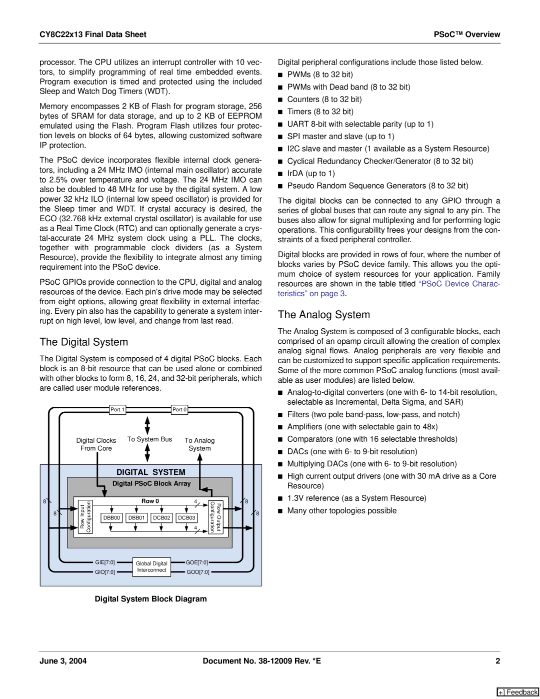
The Digital System
The Digital System is composed of 4 digital PSoC blocks. Each block is an
Port 1 |
| Port 0 |
|
|
|
Digital Clocks | To System Bus | To Analog | |
From Core |
|
| System |
|
|
|
|
|
| DIGITAL SYSTEM |
|
| |||
|
| Digital PSoC Block Array |
|
| |||
8 | Configuration |
| Row 0 | 4 | Row Output Configuration | 8 | |
8 | DBB00 | DBB01 | DCB02 | DCB03 | 8 | ||
RowInput |
| ||||||
|
|
| 4 |
| |||
|
| GIE[7:0] | Global Digital | GOE[7:0] |
|
| |
|
| GIO[7:0] | Interconnect | GOO[7:0] |
|
| |
|
|
|
|
|
| ||
Digital System Block Diagram
Digital peripheral configurations include those listed below.
■PWMs (8 to 32 bit)
■PWMs with Dead band (8 to 32 bit)
■Counters (8 to 32 bit)
■Timers (8 to 32 bit)
■UART
■SPI master and slave (up to 1)
■I2C slave and master (1 available as a System Resource)
■Cyclical Redundancy Checker/Generator (8 to 32 bit)
■IrDA (up to 1)
■Pseudo Random Sequence Generators (8 to 32 bit)
The digital blocks can be connected to any GPIO through a series of global buses that can route any signal to any pin. The buses also allow for signal multiplexing and for performing logic operations. This configurability frees your designs from the con- straints of a fixed peripheral controller.
Digital blocks are provided in rows of four, where the number of blocks varies by PSoC device family. This allows you the opti- mum choice of system resources for your application. Family resources are shown in the table titled “PSoC Device Charac- teristics” on page 3.
The Analog System
The Analog System is composed of 3 configurable blocks, each comprised of an opamp circuit allowing the creation of complex analog signal flows. Analog peripherals are very flexible and can be customized to support specific application requirements. Some of the more common PSoC analog functions (most avail- able as user modules) are listed below.
■
■Filters (two pole
■Amplifiers (one with selectable gain to 48x)
■Comparators (one with 16 selectable thresholds)
■DACs (one with 6- to
■Multiplying DACs (one with 6- to
■High current output drivers (one with 30 mA drive as a Core Resource)
■1.3V reference (as a System Resource)
■Many other topologies possible
June 3, 2004 | Document No. | 2 |
[+] Feedback