CY8C22x13 Final Data Sheet | 3. Electrical Specifications |
|
|
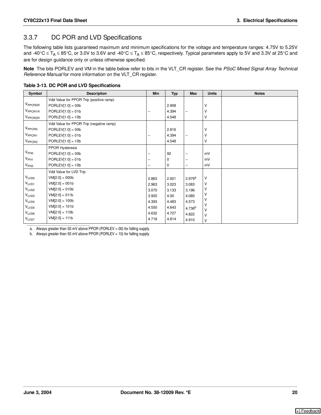
3.3.7DC POR and LVD Specifications
The following table lists guaranteed maximum and minimum specifications for the voltage and temperature ranges: 4.75V to 5.25V and
Note The bits PORLEV and VM in the table below refer to bits in the VLT_CR register. See the PSoC Mixed Signal Array Technical Reference Manual for more information on the VLT_CR register.
Table 3-13. DC POR and LVD Specifications
| Symbol | Description | Min | Typ | Max | Units | Notes | |
|
| Vdd Value for PPOR Trip (positive ramp) |
|
|
|
|
| |
VPPOR0R | PORLEV[1:0] = 00b |
| 2.908 |
| V |
| ||
VPPOR1R | PORLEV[1:0] = 01b | – | 4.394 | – | V |
| ||
VPPOR2R | PORLEV[1:0] = 10b |
| 4.548 |
| V |
| ||
|
| Vdd Value for PPOR Trip (negative ramp) |
|
|
|
|
| |
VPPOR0 | PORLEV[1:0] = 00b |
| 2.816 |
| V |
| ||
VPPOR1 | PORLEV[1:0] = 01b | – | 4.394 | – | V |
| ||
VPPOR2 | PORLEV[1:0] = 10b |
| 4.548 |
| V |
| ||
|
| PPOR Hysteresis |
|
|
|
|
| |
VPH0 | PORLEV[1:0] = 00b | – | 92 | – | mV |
| ||
VPH1 | PORLEV[1:0] = 01b | – | 0 | – | mV |
| ||
VPH2 | PORLEV[1:0] = 10b | – | 0 | – | mV |
| ||
|
| Vdd Value for LVD Trip |
|
|
|
|
| |
VLVD0 | VM[2:0] = 000b | 2.863 | 2.921 | 2.979a | V |
| ||
VLVD1 | VM[2:0] = 001b | 2.963 | 3.023 | 3.083 | V |
| ||
VLVD2 | VM[2:0] = 010b | 3.070 | 3.133 | 3.196 | V |
| ||
VLVD3 | VM[2:0] = 011b | 3.920 | 4.00 | 4.080 | V |
| ||
VLVD4 | VM[2:0] = 100b | 4.393 | 4.483 | 4.573 | V |
| ||
V |
| |||||||
VLVD5 | VM[2:0] = 101b | 4.550 | 4.643 | 4.736b |
| |||
V |
| |||||||
VLVD6 | VM[2:0] = 110b | 4.632 | 4.727 |
|
| |||
4.822 | V |
| ||||||
VLVD7 | VM[2:0] = 111b | 4.718 | 4.814 |
|
| |||
4.910 | V |
| ||||||
|
|
| ||||||
|
|
|
|
|
|
|
|
|
a.Always greater than 50 mV above PPOR (PORLEV = 00) for falling supply.
b.Always greater than 50 mV above PPOR (PORLEV = 10) for falling supply.
June 3, 2004 | Document No. | 20 |
[+] Feedback
