CYD01S36V
CYD02S36V/36VA/CYD04S36V
CYD09S36V/CYD18S36V
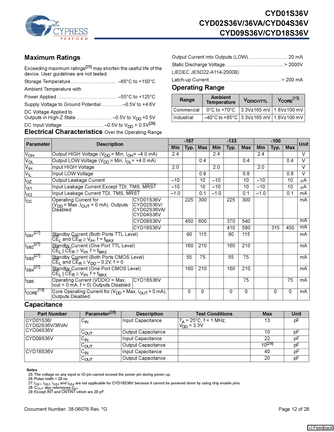
Maximum Ratings
Exceeding maximum ratings[25] may shorten the useful life of the device. User guidelines are not tested.
Storage Temperature | |
Ambient Temperature with |
|
Power Applied | |
Supply Voltage to Ground Potential | |
DC Voltage Applied to |
|
Outputs in | |
DC Input Voltage |
Electrical Characteristics Over the Operating Range
Output Current into Outputs (LOW) | 20 mA | ||
Static Discharge Voltage |
| > 2000V | |
(JEDEC |
|
| |
| > 200 mA | ||
Operating Range |
|
| |
|
|
|
|
Range | Ambient | VDDIO/VTTL | [13] |
Temperature | VCORE | ||
Commercial | 0°C to +70°C | 3.3V±165 mV | 1.8V±100 mV |
|
|
|
|
Industrial | 3.3V±165 mV | 1.8V±100 mV | |
|
|
|
|
Parameter |
| Description |
|
|
|
|
|
|
|
|
| Unit |
| |||||
|
|
| Min | Typ. | Max | Min | Typ. | Max | Min | Typ. | Max |
| ||||||
VOH | Output HIGH Voltage (VDD = Min, IOH= | 2.4 |
|
| 2.4 |
|
|
| 2.4 |
|
| V |
| |||||
VOL | Output LOW Voltage (VDD = Min, IOL= +4.0 mA) |
|
|
| 0.4 |
|
| 0.4 |
|
|
| 0.4 | V |
| ||||
VIH | Input HIGH Voltage |
|
|
| 2.0 |
|
| 2.0 |
|
|
| 2.0 |
|
| V |
| ||
VIL | Input LOW Voltage |
|
|
|
|
|
| 0.8 |
|
| 0.8 |
|
|
| 0.8 | V |
| |
IOZ | Output Leakage Current |
|
|
|
| 10 |
| 10 |
|
| 10 | μA |
| |||||
IIX1 | Input Leakage Current Except TDI, TMS, | MRST |
| 10 |
| 10 |
|
| 10 | μA |
| |||||||
IIX2 | Input Leakage Current TDI, TMS, MRST |
| 0.1 |
| 0.1 |
|
| 0.1 | mA |
| ||||||||
ICC | Operating Current for |
| CYD01S36V |
|
| 225 | 300 |
| 225 | 300 |
|
|
|
| mA |
| ||
| (VDD = Max.,IOUT = 0 mA), Outputs | CYD02S36V/ |
|
|
|
|
|
|
|
|
|
|
|
|
| |||
| Disabled |
|
| CYD02S36VA/ |
|
|
|
|
|
|
|
|
|
|
|
|
| |
|
|
|
| CYD04S36V |
|
|
|
|
|
|
|
|
|
|
|
|
| |
|
|
|
| CYD09S36V |
|
| 450 | 600 |
| 370 | 540 |
|
|
|
| mA |
| |
ISB1[27] |
|
|
| CYD18S36V |
|
|
|
|
| 410 | 580 |
|
| 315 | 450 | mA |
| |
Standby Current (Both Ports TTL Level) |
|
| 90 | 115 |
| 90 | 115 |
|
|
|
| mA |
| |||||
ISB2[27] | CEL and CER ≥ VIH, f = fMAX |
|
|
|
|
|
|
|
|
|
|
|
|
|
|
|
| |
Standby Current (One Port TTL Level) |
|
| 160 | 210 |
| 160 | 210 |
|
|
|
| mA |
| |||||
ISB3[27] | CEL CER ≥ VIH, f = fMAX |
|
|
|
|
|
|
|
|
|
|
|
|
|
|
|
| |
Standby Current (Both Ports CMOS Level) |
|
| 55 | 75 |
| 55 | 75 |
|
|
|
| mA |
| |||||
ISB4[27] | CEL and CER ≥ VDD – 0.2V, f = 0 |
|
|
|
|
|
|
|
|
|
|
|
|
|
|
| ||
Standby Current (One Port CMOS Level) |
|
| 160 | 210 |
| 160 | 210 |
|
|
|
| mA |
| |||||
| CEL CER ≥ VIH, f = fMAX |
|
|
|
|
|
|
|
|
|
|
|
|
|
|
|
| |
ISB5 | Operating Current (VDDIO = Max, | CYD18S36V |
|
|
|
|
|
| 75 |
|
|
| 75 | mA |
| |||
ICORE[13] | Iout = 0 mA, f = 0) Outputs Disabled |
|
|
|
|
|
|
|
|
|
|
|
|
|
|
| ||
Core Operating Current for (VDD = Max, IOUT = 0 mA), |
|
| 0 | 0 |
| 0 | 0 |
|
| 0 | 0 | mA |
| |||||
| Outputs Disabled |
|
|
|
|
|
|
|
|
|
|
|
|
|
|
|
| |
Capacitance |
|
|
|
|
|
|
|
|
|
|
|
|
|
|
|
|
| |
|
|
|
|
|
|
|
|
|
|
|
|
|
|
|
|
|
| |
Part Number | Parameter[28] |
| Description |
|
|
| Test Conditions |
|
| Max | Unit |
| ||||||
CYD01S36/ |
| CIN | Input Capacitance |
| TA = 25°C, f = 1 MHz, |
|
| 13 | pF |
| ||||||||
CYD02S36V/36VA/ |
|
|
|
|
| VDD = 3.3V |
|
|
|
|
|
|
|
|
| |||
CYD04S36V |
|
|
|
|
|
|
|
|
|
|
|
|
|
|
|
|
| |
COUT | Output Capacitance |
|
|
|
|
|
|
|
| 10 | pF |
| ||||||
CYD09S36V | CIN | Input Capacitance |
|
|
|
|
|
|
|
| 22 | pF |
| |||||
|
| COUT | Output Capacitance |
|
|
|
|
|
|
|
| 10[29] | pF |
| ||||
CYD18S36V | CIN | Input Capacitance |
|
|
|
|
|
|
|
| 40 | pF |
| |||||
|
| COUT | Output Capacitance |
|
|
|
|
|
|
|
| 20 | pF |
| ||||
Notes
25.The voltage on any input or IO pin cannot exceed the power pin during power up.
26.Pulse width < 20 ns.
27.ISB1, ISB2, ISB3 and ISB4 are not applicable for CYD18S36V because it cannot be powered down by using chip enable pins.
28.COUT also references CIO.
29.Except INT and CNTINT which are 20 pF.
Document Number: | Page 12 of 28 |
[+] Feedback