CYD01S36V
CYD02S36V/36VA/CYD04S36V
CYD09S36V/CYD18S36V
Switching Waveforms (continued)
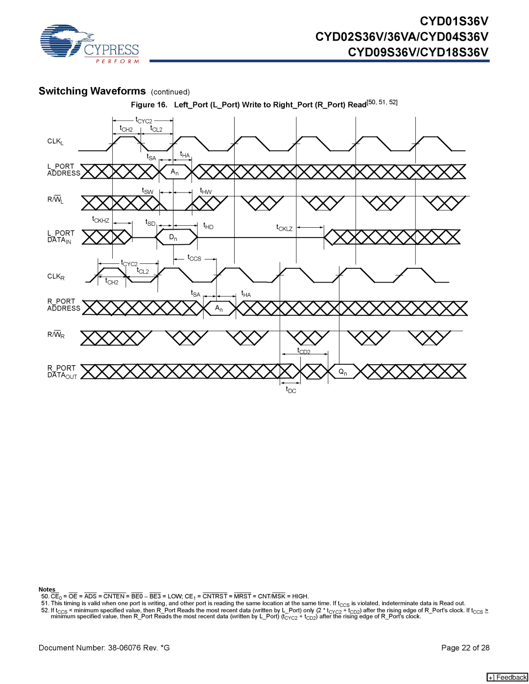
Figure 16. Left_Port (L_Port) Write to Right_Port (R_Port) Read[50, 51, 52]
|
|
|
|
|
|
|
| tCYC2 |
|
|
|
|
|
|
|
|
|
|
|
|
| ||||||||||
|
|
|
|
|
|
|
|
|
|
|
|
|
|
|
|
|
|
|
| ||||||||||||
|
|
|
|
|
|
|
|
|
|
|
|
|
|
|
|
|
|
|
|
| |||||||||||
CLKL |
|
| tCH2 |
|
|
|
|
|
|
| tCL2 |
|
|
|
|
|
|
|
|
|
|
|
| ||||||||
|
|
|
|
|
|
|
|
|
|
|
|
|
|
|
|
|
|
|
|
| |||||||||||
|
|
|
|
|
|
|
|
|
|
|
|
|
|
|
|
|
|
|
|
|
|
|
|
|
|
|
| ||||
|
|
|
|
|
|
|
|
|
|
|
|
|
|
|
|
|
|
|
|
|
| tHA |
|
| |||||||
|
|
|
|
|
|
|
|
|
|
|
|
|
|
|
|
|
|
|
|
|
|
|
| ||||||||
|
|
|
|
|
|
|
|
|
|
|
|
|
|
|
|
|
|
|
|
|
|
|
|
|
|
| |||||
L_PORT |
|
|
|
|
|
|
|
|
|
|
|
| tSA |
|
|
|
|
|
|
|
|
|
| ||||||||
|
|
|
|
|
|
|
|
|
|
|
|
|
|
|
|
| |||||||||||||||
|
|
|
|
|
|
|
|
|
|
|
|
|
|
|
|
|
|
|
|
|
|
|
|
| |||||||
|
|
|
|
|
|
|
|
|
|
|
|
|
|
|
| An |
|
| |||||||||||||
ADDRESS |
|
|
|
|
|
|
|
|
|
|
|
|
|
|
|
|
| ||||||||||||||
|
|
|
|
|
|
|
|
|
|
|
|
|
|
|
|
|
|
|
|
|
|
|
|
|
|
|
|
|
|
|
|
R/WL | tSW | tHW |
|
|
|
| |
tCKHZ | tSD | tHD | tCKLZ |
L_PORT |
| ||
| Dn |
| |
DATAIN |
|
|
|
|
|
|
|
|
|
|
|
| tCYC2 |
|
|
|
|
|
|
|
|
|
| tCCS |
|
|
|
|
|
|
|
|
|
|
| ||||||||||
|
|
|
|
|
|
|
|
|
|
|
|
|
|
|
|
|
|
|
|
|
|
|
|
|
|
|
|
|
|
| ||||||||||||
|
|
|
|
|
|
|
|
|
|
|
|
|
|
|
|
|
|
|
|
|
|
|
|
|
| |||||||||||||||||
CLKR |
|
|
|
|
|
|
|
|
|
|
|
| tCL2 |
|
|
|
|
|
|
|
|
|
|
|
|
|
|
|
|
|
|
|
|
|
| |||||||
|
|
|
|
|
|
|
|
|
|
|
|
|
|
|
|
|
| |||||||||||||||||||||||||
|
|
|
|
|
|
|
|
|
|
|
|
|
|
|
|
|
|
|
|
|
|
|
|
|
|
|
|
|
|
|
|
|
|
|
|
|
|
| ||||
|
|
|
| tCH2 |
|
|
|
|
|
|
|
|
|
|
|
|
|
|
|
|
|
|
|
|
|
|
|
|
|
|
|
|
|
|
| |||||||
R_PORT |
|
|
|
|
|
|
|
|
|
|
|
|
|
|
|
|
|
|
| tSA |
|
|
|
|
|
|
|
|
|
|
|
|
| tHA | ||||||||
|
|
|
|
|
|
|
|
|
|
|
|
|
|
|
|
|
|
|
|
|
|
|
|
|
|
|
|
|
|
|
|
|
|
|
|
|
| |||||
|
|
|
|
|
|
|
|
|
|
|
|
|
|
|
|
|
|
|
|
|
|
|
|
|
|
|
|
|
|
|
|
|
|
|
|
| ||||||
|
|
|
|
|
|
|
|
|
|
|
|
|
|
|
|
|
|
|
|
|
|
|
|
|
|
|
|
| An |
|
|
| ||||||||||
ADDRESS |
|
|
|
|
|
|
|
|
|
|
|
|
|
|
|
|
|
|
|
|
|
|
|
|
|
|
| |||||||||||||||
|
|
|
|
|
|
|
|
|
|
|
|
|
|
|
|
|
|
|
|
|
|
|
|
|
|
|
|
|
|
|
|
|
|
|
|
|
|
|
|
|
|
|
R/WR |
|
| tCD2 |
R_PORT | Qn |
DATAOUT | |
| tDC |
Notes
50.CE0 = OE = ADS = CNTEN = BE0 – BE3 = LOW; CE1 = CNTRST = MRST = CNT/MSK = HIGH.
51.This timing is valid when one port is writing, and other port is reading the same location at the same time. If tCCS is violated, indeterminate data is Read out.
52.If tCCS < minimum specified value, then R_Port Reads the most recent data (written by L_Port) only (2 * tCYC2 + tCD2) after the rising edge of R_Port's clock. If tCCS > minimum specified value, then R_Port Reads the most recent data (written by L_Port) (tCYC2 + tCD2) after the rising edge of R_Port's clock.
Document Number: | Page 22 of 28 |
[+] Feedback