CYD01S36V
CYD02S36V/36VA/CYD04S36V
CYD09S36V/CYD18S36V
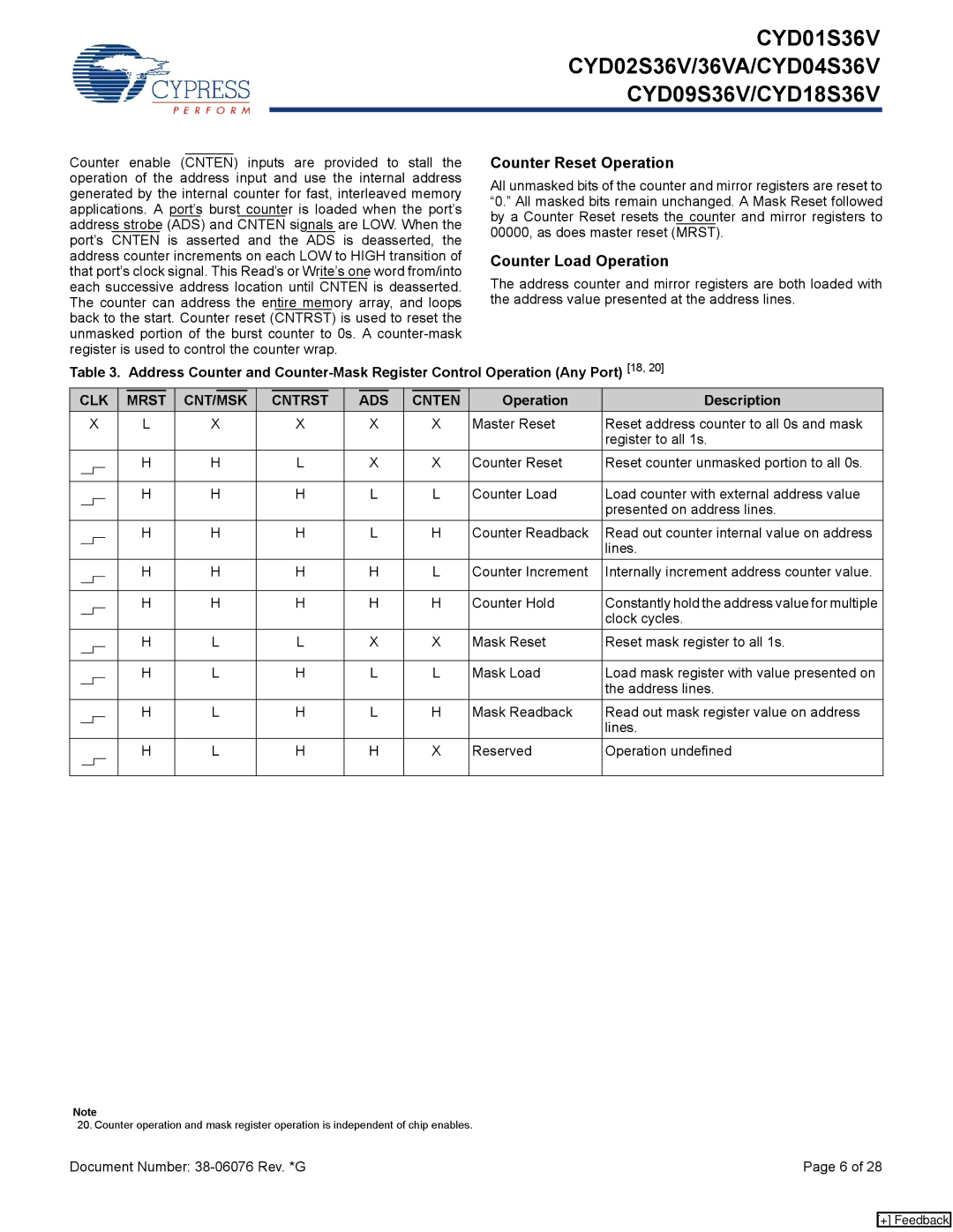
Counter enable (CNTEN) inputs are provided to stall the operation of the address input and use the internal address generated by the internal counter for fast, interleaved memory applications. A port’s burst counter is loaded when the port’s address strobe (ADS) and CNTEN signals are LOW. When the port’s CNTEN is asserted and the ADS is deasserted, the address counter increments on each LOW to HIGH transition of that port’s clock signal. This Read’s or Write’s one word from/into each successive address location until CNTEN is deasserted. The counter can address the entire memory array, and loops back to the start. Counter reset (CNTRST) is used to reset the unmasked portion of the burst counter to 0s. A
Counter Reset Operation
All unmasked bits of the counter and mirror registers are reset to “0.” All masked bits remain unchanged. A Mask Reset followed by a Counter Reset resets the counter and mirror registers to 00000, as does master reset (MRST).
Counter Load Operation
The address counter and mirror registers are both loaded with the address value presented at the address lines.
Table 3. Address Counter and
CLK | MRST | CNT/MSK | CNTRST | ADS | CNTEN | Operation | Description | |||
| X | L | X | X | X | X | Master Reset | Reset address counter to all 0s and mask | ||
|
|
|
|
|
|
|
|
|
| register to all 1s. |
|
|
|
| H | H | L | X | X | Counter Reset | Reset counter unmasked portion to all 0s. |
|
|
|
|
|
|
|
|
|
|
|
|
|
|
|
|
|
|
|
|
|
|
|
|
|
| H | H | H | L | L | Counter Load | Load counter with external address value |
|
|
|
|
|
|
|
|
|
| presented on address lines. |
|
|
|
|
|
|
|
|
|
| |
|
|
|
| H | H | H | L | H | Counter Readback | Read out counter internal value on address |
|
|
|
|
|
|
|
|
|
| lines. |
|
|
|
|
|
|
|
|
|
| |
|
|
|
| H | H | H | H | L | Counter Increment | Internally increment address counter value. |
|
|
|
|
|
|
|
|
|
|
|
|
|
|
|
|
|
|
|
|
|
|
|
|
|
| H | H | H | H | H | Counter Hold | Constantly hold the address value for multiple |
|
|
|
|
|
|
|
|
|
| clock cycles. |
|
|
|
|
|
|
|
|
|
| |
|
|
|
| H | L | L | X | X | Mask Reset | Reset mask register to all 1s. |
|
|
|
|
|
|
|
|
|
|
|
|
|
|
|
|
|
|
|
|
|
|
|
|
|
| H | L | H | L | L | Mask Load | Load mask register with value presented on |
|
|
|
|
|
|
|
|
|
| the address lines. |
|
|
|
|
|
|
|
|
|
| |
|
|
|
| H | L | H | L | H | Mask Readback | Read out mask register value on address |
|
|
|
|
|
|
|
|
|
| lines. |
|
|
|
|
|
|
|
|
|
| |
|
|
|
| H | L | H | H | X | Reserved | Operation undefined |
|
|
|
|
|
|
|
|
|
|
|
|
|
|
|
|
|
|
|
|
|
|
Note
20. Counter operation and mask register operation is independent of chip enables.
Document Number: | Page 6 of 28 |
[+] Feedback