CYD01S36V
CYD02S36V/36VA/CYD04S36V
CYD09S36V/CYD18S36V
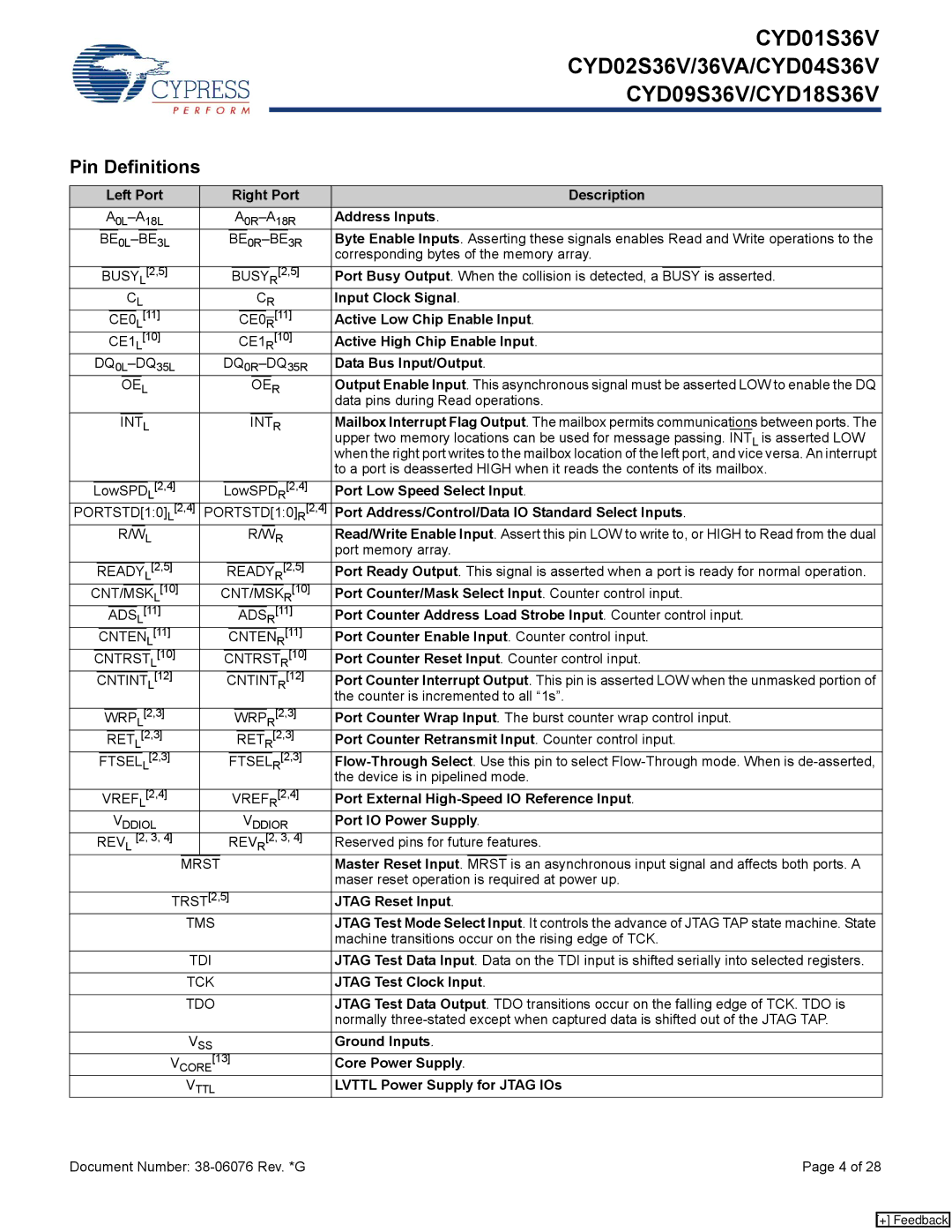
Pin Definitions
|
|
|
|
| Left Port |
|
|
|
|
|
|
|
|
|
|
| Right Port |
|
| Description | |||||||||||||||||||||||||||||||||||||||||||||||
|
|
|
|
|
|
|
|
|
|
|
|
|
|
|
|
| Address Inputs. | ||||||||||||||||||||||||||||||||||||||||||||||||||
|
|
| BE | 3L |
|
|
|
|
|
|
|
| BE | 3R | Byte Enable Inputs. Asserting these signals enables Read and Write operations to the | ||||||||||||||||||||||||||||||||||||||||||||||||||||
|
|
|
|
|
|
|
|
|
|
|
|
|
|
|
|
|
|
|
|
|
|
|
|
|
|
|
|
|
|
|
|
|
|
|
|
|
|
|
|
|
|
|
|
|
|
|
|
|
|
|
|
|
|
|
|
|
|
|
|
|
|
| corresponding bytes of the memory array. | ||||
|
|
|
| BUSY |
|
| [2,5] |
|
|
|
|
|
|
|
|
|
| BUSY |
|
| [2,5] | Port Busy Output. When the collision is detected, a | BUSY | is asserted. | |||||||||||||||||||||||||||||||||||||||||||
|
|
|
|
|
|
|
|
|
|
|
|
|
|
| L |
|
|
|
|
|
|
|
|
|
|
|
|
|
|
|
|
|
|
|
|
|
|
|
|
|
|
| R |
|
|
|
|
|
|
|
| ||||||||||||||||
|
|
|
|
|
|
|
|
|
| CL |
|
|
|
|
|
|
|
|
|
|
|
|
|
|
|
|
|
|
|
|
| CR |
|
|
| Input Clock Signal. | |||||||||||||||||||||||||||||||
|
|
|
|
|
|
| CE0 | L | [11] |
|
|
|
|
|
|
|
|
|
|
|
|
|
|
| CE0 |
|
|
|
| [11] | Active Low Chip Enable Input. | ||||||||||||||||||||||||||||||||||||
|
|
|
|
|
|
|
|
|
|
|
|
|
|
|
|
|
|
|
|
|
|
|
|
|
|
|
| ||||||||||||||||||||||||||||||||||||||||
|
|
|
|
|
|
|
|
|
|
|
|
|
|
|
|
|
|
|
|
|
|
|
|
|
|
|
|
|
|
|
|
|
|
|
|
|
|
|
|
|
|
|
|
| R |
|
|
|
|
|
|
|
| ||||||||||||||
|
|
|
|
|
|
| CE1 | [10] |
|
|
|
|
|
|
|
|
|
|
|
|
|
| CE1 | [10] | Active High Chip Enable Input. | ||||||||||||||||||||||||||||||||||||||||||
|
|
|
|
|
|
|
|
|
|
|
| L |
|
|
|
|
|
|
|
|
|
|
|
|
|
|
|
|
|
|
|
|
|
|
|
|
|
|
|
|
|
|
| R |
|
|
|
|
|
|
|
| |||||||||||||||
|
| Data Bus Input/Output. | |||||||||||||||||||||||||||||||||||||||||||||||||||||||||||||||||
|
|
|
|
|
|
|
|
| OE | L |
|
|
|
|
|
|
|
|
|
|
|
|
|
|
|
|
|
|
|
| OE | R |
|
|
| Output Enable Input. This asynchronous signal must be asserted LOW to enable the DQ | |||||||||||||||||||||||||||||||
|
|
|
|
|
|
|
|
|
|
|
|
|
|
|
|
|
|
|
|
|
|
|
|
|
|
|
|
|
|
|
|
|
|
|
|
|
|
|
|
|
|
|
|
|
|
|
|
|
|
|
|
|
|
|
|
|
|
|
|
|
|
| data pins during Read operations. | ||||
|
|
|
|
|
|
|
|
| INT | L |
|
|
|
|
|
|
|
|
|
|
|
|
|
|
|
|
|
|
| INT | R | Mailbox Interrupt Flag Output. The mailbox permits communications between ports. The | |||||||||||||||||||||||||||||||||||
|
|
|
|
|
|
|
|
|
|
|
|
|
|
|
|
|
|
|
|
|
|
|
|
|
|
|
|
|
|
|
|
|
|
|
|
|
|
|
|
|
|
|
|
|
|
|
|
|
|
|
|
|
|
|
|
|
|
|
|
|
|
| upper two memory locations can be used for message passing. INTL is asserted LOW | ||||
|
|
|
|
|
|
|
|
|
|
|
|
|
|
|
|
|
|
|
|
|
|
|
|
|
|
|
|
|
|
|
|
|
|
|
|
|
|
|
|
|
|
|
|
|
|
|
|
|
|
|
|
|
|
|
|
|
|
|
|
|
|
| when the right port writes to the mailbox location of the left port, and vice versa. An interrupt | ||||
|
|
|
|
|
|
|
|
|
|
|
|
|
|
|
|
|
|
|
|
|
|
|
|
|
|
|
|
|
|
|
|
|
|
|
|
|
|
|
|
|
|
|
|
|
|
|
|
|
|
|
|
|
|
|
|
|
|
|
|
|
|
| to a port is deasserted HIGH when it reads the contents of its mailbox. | ||||
| LowSPD | [2,4] |
|
|
| LowSPD |
| [2,4] | Port Low Speed Select Input. | ||||||||||||||||||||||||||||||||||||||||||||||||||||||||||
|
|
|
|
|
|
|
|
|
|
|
|
|
|
|
|
|
|
|
|
|
| L |
|
|
|
|
|
|
|
|
|
|
|
|
|
|
|
|
|
|
|
|
|
|
|
|
|
|
|
|
|
|
|
|
|
| R |
|
|
|
|
| |||||
PORTSTD[1:0] | L | [2,4] | PORTSTD[1:0] [2,4] | Port Address/Control/Data IO Standard Select Inputs. | |||||||||||||||||||||||||||||||||||||||||||||||||||||||||||||||
|
|
|
|
|
|
|
|
|
|
|
|
|
|
|
|
|
|
|
|
|
|
|
|
|
|
|
|
|
|
|
|
|
|
|
|
|
|
|
|
|
|
|
|
|
|
|
|
|
|
|
|
|
|
|
|
|
|
|
|
| R |
|
|
|
|
| |
|
|
|
|
|
|
| R/W | L |
|
|
|
|
|
|
|
|
|
|
|
|
|
|
|
|
|
| R/W | R | Read/Write Enable Input. Assert this pin LOW to write to, or HIGH to Read from the dual | ||||||||||||||||||||||||||||||||||||||
|
|
|
|
|
|
|
|
|
|
|
|
|
|
|
|
|
|
|
|
|
|
|
|
|
|
|
|
|
|
|
|
|
|
|
|
|
|
|
|
|
|
|
|
|
|
|
|
|
|
|
|
|
|
|
|
|
|
|
|
|
|
| port memory array. | ||||
|
| READY | L[2,5] |
|
|
|
|
|
| READY | R[2,5] | Port Ready Output. This signal is asserted when a port is ready for normal operation. | |||||||||||||||||||||||||||||||||||||||||||||||||||||||
CNT/MSK | L | [10] |
|
| CNT/MSK | [10] | Port Counter/Mask Select Input. Counter control input. | ||||||||||||||||||||||||||||||||||||||||||||||||||||||||||||
|
|
|
|
|
|
|
|
|
|
|
|
|
|
|
|
|
|
|
|
|
|
|
|
|
|
|
|
|
|
|
|
|
|
|
|
|
|
|
|
|
|
|
|
|
|
|
|
|
|
|
|
|
|
|
|
|
|
| R |
|
|
|
|
| |||
|
|
|
|
|
|
| ADS | L[11] |
|
|
|
|
|
|
|
|
|
|
|
|
|
| ADS | R[11] | Port Counter Address Load Strobe Input. Counter control input. | ||||||||||||||||||||||||||||||||||||||||||
|
|
| CNTEN | [11] |
|
|
|
|
|
|
| CNTEN |
| [11] | Port Counter Enable Input. Counter control input. | ||||||||||||||||||||||||||||||||||||||||||||||||||||
|
|
|
|
|
|
|
|
|
|
|
|
|
|
|
|
|
|
|
|
| L |
|
|
|
|
|
|
|
|
|
|
|
|
|
|
|
|
|
|
|
|
|
|
|
|
|
|
|
|
|
|
|
|
| R |
|
|
|
|
| |||||||
| CNTRST | L | [10] |
|
|
|
| CNTRST | [10] | Port Counter Reset Input. Counter control input. | |||||||||||||||||||||||||||||||||||||||||||||||||||||||||
|
|
|
|
|
|
|
|
|
|
|
|
|
|
|
|
|
|
|
|
|
|
|
|
|
|
|
|
|
|
|
|
|
|
|
|
|
|
|
|
|
|
|
|
|
|
|
|
|
|
|
|
|
|
|
|
|
| R |
|
|
|
|
| ||||
|
| CNTINT | [12] |
|
|
|
|
|
| CNTINT |
| [12] | Port Counter Interrupt Output. This pin is asserted LOW when the unmasked portion of | ||||||||||||||||||||||||||||||||||||||||||||||||||||||
|
|
|
|
|
|
|
|
|
|
|
|
|
|
|
|
|
|
|
|
|
| L |
|
|
|
|
|
|
|
|
|
|
|
|
|
|
|
|
|
|
|
|
|
|
|
|
|
|
|
|
|
|
|
|
|
| R | the counter is incremented to all “1s”. | |||||||||
|
|
|
|
|
|
|
|
|
|
|
|
|
|
|
|
|
|
|
|
|
|
|
|
|
|
|
|
|
|
|
|
|
|
|
|
|
|
|
|
|
|
|
|
|
|
|
|
|
|
|
|
|
|
|
|
|
|
|
|
|
|
| |||||
|
|
|
|
|
|
|
|
|
|
|
|
|
|
|
|
|
|
|
|
|
|
|
|
|
| ||||||||||||||||||||||||||||||||||||||||||
|
|
|
|
| WRP | L[2,3] |
|
|
|
|
|
|
|
|
|
|
|
| WRP | R[2,3] | Port Counter Wrap Input. The burst counter wrap control input. | ||||||||||||||||||||||||||||||||||||||||||||||
|
|
|
|
|
| RET |
| [2,3] |
|
|
|
|
|
|
|
|
|
|
|
|
| RET |
| [2,3] | Port Counter Retransmit Input. Counter control input. | ||||||||||||||||||||||||||||||||||||||||||
|
|
|
|
|
|
|
|
|
|
| L |
|
|
|
|
|
|
|
|
|
|
|
|
|
|
|
|
|
|
|
|
|
|
|
|
|
|
|
|
|
|
| R |
|
|
|
|
|
|
|
| ||||||||||||||||
|
|
| FTSEL | [2,3] |
|
|
|
|
|
|
|
|
| FTSEL | R | [2,3] | |||||||||||||||||||||||||||||||||||||||||||||||||||
|
|
|
|
|
|
|
|
|
|
|
|
|
|
|
|
| L |
|
|
|
|
|
|
|
|
|
|
|
|
|
|
|
|
|
|
|
|
|
|
|
|
|
|
|
|
|
|
|
| the device is in pipelined mode. | |||||||||||||||||
|
|
|
|
|
|
|
|
|
|
|
|
|
|
|
|
|
|
|
|
|
|
|
|
|
|
|
|
|
|
|
|
|
|
|
|
|
|
|
|
|
|
|
|
|
|
|
|
|
|
|
|
|
|
|
|
|
|
|
|
|
|
| |||||
|
|
|
|
|
|
|
|
|
|
|
|
|
|
|
|
|
|
|
| ||||||||||||||||||||||||||||||||||||||||||||||||
|
|
|
| VREF | [2,4] |
|
|
|
|
|
|
|
|
|
|
| VREF | [2,4] | Port External | ||||||||||||||||||||||||||||||||||||||||||||||||
|
|
|
|
|
|
|
|
|
|
|
|
|
| L |
|
|
|
|
|
|
|
|
|
|
|
|
|
|
|
|
|
|
|
|
|
|
|
|
| R |
|
|
|
|
|
|
|
| |||||||||||||||||||
|
|
|
|
|
|
| VDDIOL |
|
|
|
|
|
|
|
|
|
|
|
|
|
|
|
|
| VDDIOR | Port IO Power Supply. | |||||||||||||||||||||||||||||||||||||||||
|
| REVL [2, 3, 4] |
|
|
|
|
|
|
| REVR[2, 3, 4] | Reserved pins for future features. | ||||||||||||||||||||||||||||||||||||||||||||||||||||||||
|
|
|
|
|
|
|
|
|
|
|
|
|
|
|
|
|
|
|
|
|
|
|
|
|
|
|
|
| MRST |
|
|
|
|
|
|
|
|
|
|
|
|
|
|
|
|
|
|
|
|
|
|
|
|
|
|
|
|
|
|
|
| Master Reset Input. | MRST | is an asynchronous input signal and affects both ports. A | |||
|
|
|
|
|
|
|
|
|
|
|
|
|
|
|
|
|
|
|
|
|
|
|
|
|
|
|
|
|
|
|
|
|
|
|
|
|
|
|
|
|
|
|
|
|
|
|
|
|
|
|
|
|
|
|
|
|
|
|
|
|
|
| maser reset operation is required at power up. | ||||
|
|
|
|
|
|
|
|
|
|
|
|
|
|
|
|
|
|
|
|
|
|
|
|
|
|
| TRST[2,5] |
|
|
|
|
|
|
|
|
| JTAG Reset Input. | ||||||||||||||||||||||||||||||
|
|
|
|
|
|
|
|
|
|
|
|
|
|
|
|
|
|
|
|
|
|
|
|
|
|
|
|
| TMS |
|
|
|
|
|
|
|
|
|
|
|
|
|
|
|
|
|
|
|
|
|
|
|
|
|
|
|
|
|
|
|
| JTAG Test Mode Select Input. It controls the advance of JTAG TAP state machine. State | |||||
|
|
|
|
|
|
|
|
|
|
|
|
|
|
|
|
|
|
|
|
|
|
|
|
|
|
|
|
|
|
|
|
|
|
|
|
|
|
|
|
|
|
|
|
|
|
|
|
|
|
|
|
|
|
|
|
|
|
|
|
|
|
| machine transitions occur on the rising edge of TCK. | ||||
|
|
|
|
|
|
|
|
|
|
|
|
|
|
|
|
|
|
|
|
|
|
|
|
|
|
|
|
| TDI |
|
|
|
|
|
|
|
|
|
|
|
|
|
|
|
|
|
|
|
|
|
|
|
|
|
|
|
|
|
|
|
| JTAG Test Data Input. Data on the TDI input is shifted serially into selected registers. | |||||
|
|
|
|
|
|
|
|
|
|
|
|
|
|
|
|
|
|
|
|
|
|
|
|
|
|
|
|
|
|
|
|
|
|
|
|
|
|
|
|
|
|
|
|
|
|
|
|
|
|
|
|
|
|
|
|
|
|
|
|
|
|
| |||||
|
|
|
|
|
|
|
|
|
|
|
|
|
|
|
|
|
|
|
|
|
|
|
|
|
|
|
|
| TCK |
|
|
|
|
|
|
|
|
|
|
|
|
|
|
|
|
|
|
|
|
|
|
|
|
|
|
|
|
|
|
|
| JTAG Test Clock Input. | |||||
|
|
|
|
|
|
|
|
|
|
|
|
|
|
|
|
|
|
|
|
|
|
|
|
|
|
|
|
| TDO |
|
|
|
|
|
|
|
|
|
|
|
|
|
|
|
|
|
|
|
|
|
|
|
|
|
|
|
|
|
|
|
| JTAG Test Data Output. TDO transitions occur on the falling edge of TCK. TDO is | |||||
|
|
|
|
|
|
|
|
|
|
|
|
|
|
|
|
|
|
|
|
|
|
|
|
|
|
|
|
|
|
|
|
|
|
|
|
|
|
|
|
|
|
|
|
|
|
|
|
|
|
|
|
|
|
|
|
|
|
|
|
|
|
| normally | ||||
|
|
|
|
|
|
|
|
|
|
|
|
|
|
|
|
|
|
|
|
|
|
|
|
|
|
|
|
| VSS |
|
|
|
|
|
|
|
|
|
|
|
|
|
|
|
|
|
|
|
|
|
|
|
|
|
|
|
|
|
|
|
| Ground Inputs. | |||||
|
|
|
|
|
|
|
|
|
|
|
|
|
|
|
|
|
|
|
|
|
|
|
|
|
|
| VCORE[13] |
|
|
|
|
|
|
|
|
| Core Power Supply. | ||||||||||||||||||||||||||||||
|
|
|
|
|
|
|
|
|
|
|
|
|
|
|
|
|
|
|
|
|
|
|
|
|
|
|
|
| VTTL |
|
|
|
|
|
|
|
|
|
|
|
|
|
|
|
|
|
|
|
|
|
|
|
|
|
|
|
|
|
|
|
| LVTTL Power Supply for JTAG IOs | |||||
Document Number: |
|
|
|
| Page 4 of 28 | ||||||||||||||||||||||||||||||||||||||||||||||||||||||||||||||
[+] Feedback