|
|
|
|
|
| CYD01S36V |
|
|
|
| CYD02S36V/36VA/CYD04S36V | ||
|
|
|
|
| CYD09S36V/CYD18S36V | |
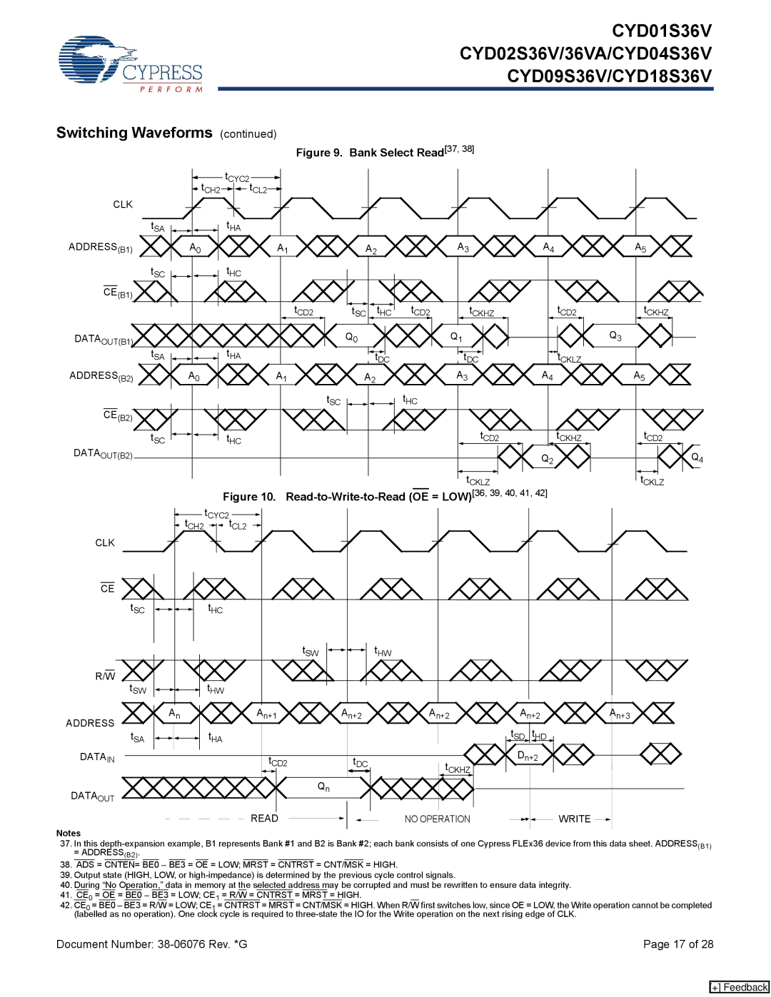
Switching Waveforms (continued) | Figure 9. Bank Select Read[37, 38] |
|
| |||
|
|
|
|
| ||
| tCH2 | tCYC2 |
|
|
|
|
| tCL2 |
|
|
|
| |
CLK |
|
|
|
|
|
|
| tSA | tHA |
|
|
|
|
ADDRESS(B1) | A0 | A1 | A2 | A3 | A4 | A5 |
| tSC | tHC |
|
|
|
|
|
|
| |
CE(B1) |
|
|
|
|
|
|
|
|
|
|
|
|
| tCD2 | tSC | tHC | tCD2 | tCKHZ | tCD2 | tCKHZ | |
DATAOUT(B1) |
|
|
| Q | 0 |
| Q |
|
| Q3 |
tSA | tHA |
|
| 1 |
|
|
| |||
|
|
| tDC | tDC | tCKLZ |
| ||||
ADDRESS(B2) | A0 |
| A1 |
| A2 | A3 | A4 |
| A5 | |
|
|
|
| tSC |
|
| tHC |
|
|
|
CE(B2) |
|
|
|
|
|
|
|
|
|
|
DATAOUT(B2) | tSC | tHC |
|
|
|
| tCD2 | tCKHZ | tCD2 | |
|
|
|
|
|
|
| Q2 |
| Q4 | |
|
|
|
|
|
|
|
|
| ||
|
|
|
|
|
|
| tCKLZ |
| tCKLZ | |
|
| Figure 10. |
|
| ||||||
| tCH2 | tCYC2 | tCL2 |
|
|
|
|
|
|
|
|
|
|
|
|
|
|
|
| ||
CLK |
|
|
|
|
|
|
|
|
|
|
CE |
|
|
|
|
|
|
|
|
|
|
tSC |
| tHC |
|
|
|
|
|
|
|
|
| tSW |
| tHW |
|
|
R/W |
|
|
|
|
|
tSW | tHW |
|
|
|
|
An | An+1 | An+2 | An+2 | An+2 | An+3 |
ADDRESS |
|
|
| tSD tHD |
|
tSA | tHA |
|
|
| |
DATA | tCD2 |
|
| Dn+2 |
|
IN | tDC | tCKHZ |
|
| |
|
|
| |||
DATAOUT | Qn |
|
|
|
|
|
|
|
|
| |
| READ |
| NO OPERATION |
| WRITE |
Notes
37.In this
38.ADS = CNTEN= BE0 – BE3 = OE = LOW; MRST = CNTRST = CNT/MSK = HIGH.
39.Output state (HIGH, LOW, or
40.During “No Operation,” data in memory at the selected address may be corrupted and must be rewritten to ensure data integrity.
41.CE0 = OE = BE0 – BE3 = LOW; CE1 = R/W = CNTRST = MRST = HIGH.
42.CE0 = BE0 – BE3 = R/W = LOW; CE1 = CNTRST = MRST = CNT/MSK = HIGH. When R/W first switches low, since OE = LOW, the Write operation cannot be completed (labelled as no operation). One clock cycle is required to
Document Number: | Page 17 of 28 |
[+] Feedback