|
|
|
|
|
|
|
|
|
|
|
|
|
| CYD01S36V |
|
|
|
|
|
| CYD02S36V/36VA/CYD04S36V | ||||||||
|
|
|
|
|
|
|
| CYD09S36V/CYD18S36V | ||||||
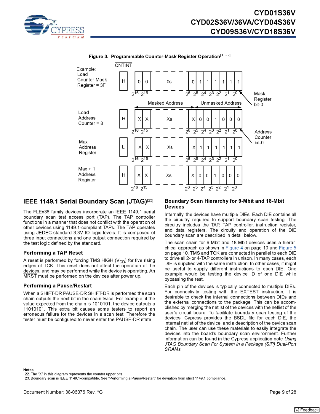
Figure 3. Programmable |
|
|
| |||||||||||
Example: | CNTINT |
|
|
|
|
|
|
|
|
|
|
|
| |
|
|
|
|
|
|
|
|
|
|
|
|
|
| |
Load |
|
|
|
|
|
|
|
|
|
|
|
|
|
|
H | 0 | 0 | 0s |
| 0 | 1 | 1 | 1 | 1 | 1 |
| 1 |
| |
Register = 3F |
|
|
|
|
|
|
|
|
|
|
|
|
|
|
|
| 216 | 215 |
| 26 | 25 | 24 | 23 | 22 | 21 |
| 20 |
| Mask |
|
|
| Masked Address |
|
| Unmasked Address | Register | |||||||
|
|
|
|
| ||||||||||
|
|
|
|
|
|
|
|
|
|
|
|
|
| |
Load |
|
|
|
|
|
|
|
|
|
|
|
|
|
|
Address | H | X | X | Xs |
| X | 0 | 0 | 1 | 0 | 0 |
| 0 |
|
Counter = 8 |
|
|
|
|
|
|
|
|
|
|
|
|
|
|
|
| 216 | 215 |
| 26 | 25 | 24 | 23 | 22 | 21 |
| 20 |
| Address |
Max |
|
|
|
|
|
|
|
|
|
|
|
|
| Counter |
L | X X | Xs |
| X | 1 | 1 | 1 | 1 | 1 | 1 | ||||
Address |
|
| ||||||||||||
Register |
|
|
|
|
|
|
|
|
|
|
|
|
|
|
|
| 216 | 215 |
| 26 | 25 | 24 | 23 | 22 | 21 |
| 20 |
|
|
Max + 1 |
|
|
|
|
|
|
|
|
|
|
|
|
|
|
Address | H | X | X | Xs |
| X | 0 | 0 | 1 | 0 0 | 0 |
| ||
Register |
|
|
|
|
|
|
|
|
|
|
|
|
|
|
|
| 216 | 215 |
| 26 | 25 | 24 | 23 | 22 | 21 |
| 20 |
|
|
IEEE 1149.1 Serial Boundary Scan (JTAG)[23]
The FLEx36 family devices incorporate an IEEE 1149.1 serial boundary scan test access port (TAP). The TAP controller functions in a manner that does not conflict with the operation of other devices using
Performing a TAP Reset
A reset is performed by forcing TMS HIGH (VDD) for five rising edges of TCK. This reset does not affect the operation of the devices, and may be performed while the device is operating. An MRST must be performed on the devices after power up.
Performing a Pause/Restart
When a
Boundary Scan Hierarchy for 9-Mbit and 18-Mbit Devices
Internally, the devices have multiple DIEs. Each DIE contains all the circuitry required to support boundary scan testing. The circuitry includes the TAP, TAP controller, instruction register, and data registers. The circuity and operation of the DIE boundary scan are described in detail below.
The scan chain for
Each pin of the devices is typically connected to multiple DIEs. For connectivity testing with the EXTEST instruction, it is desirable to check the internal connections between DIEs and the external connections to the package. This can be accom- plished by merging the netlist of the devices with the netlist of the user’s circuit board. To facilitate boundary scan testing of the devices, Cypress provides the BSDL file for each DIE, the internal netlist of the device, and a description of the device scan chain. The user can use these materials to easily integrate the devices into the board’s boundary scan environment. Further information can be found in the Cypress application note Using JTAG Boundary Scan For System in a Package (SIP)
Notes
22.The “X” in this diagram represents the counter upper bits.
23.Boundary scan is IEEE
Document Number: | Page 9 of 28 |
[+] Feedback