CYD01S36V
CYD02S36V/36VA/CYD04S36V
CYD09S36V/CYD18S36V
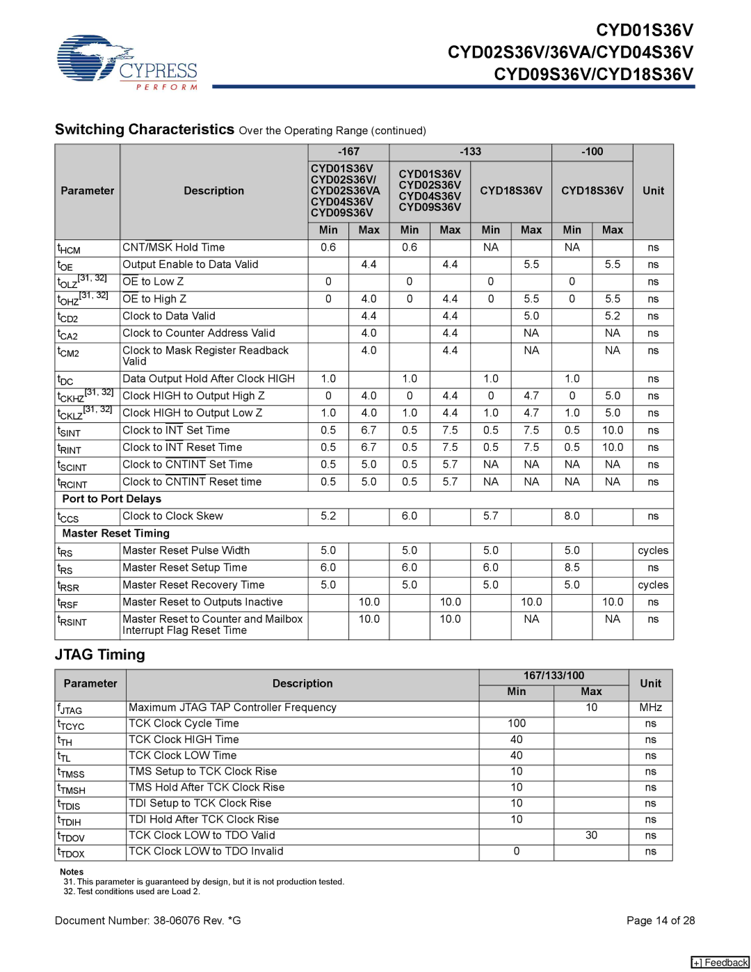
Switching Characteristics Over the Operating Range (continued)
|
|
|
|
|
|
|
|
|
|
|
|
|
| ||||||
|
|
|
|
|
|
|
|
|
|
| CYD01S36V | CYD01S36V |
|
|
|
|
| ||
|
|
|
|
|
|
|
|
|
|
| CYD02S36V/ |
|
|
|
|
| |||
|
|
|
|
|
|
|
|
|
|
| CYD02S36V |
|
|
|
|
| |||
Parameter |
|
|
|
|
|
|
| Description | CYD02S36VA | CYD18S36V | CYD18S36V | Unit | |||||||
|
|
|
|
|
|
| CYD04S36V | ||||||||||||
|
|
|
|
|
|
|
|
|
|
| CYD04S36V |
|
|
|
|
| |||
|
|
|
|
|
|
|
|
|
|
| CYD09S36V |
|
|
|
|
| |||
|
|
|
|
|
|
|
|
|
|
| CYD09S36V |
|
|
|
|
| |||
|
|
|
|
|
|
|
|
|
|
|
|
|
|
|
|
|
| ||
|
|
|
|
|
|
|
|
|
|
| Min | Max | Min | Max | Min | Max | Min | Max |
|
tHCM |
|
| CNT/MSK | Hold Time | 0.6 |
| 0.6 |
| NA |
| NA |
| ns | ||||||
tOE |
|
| Output Enable to Data Valid |
| 4.4 |
| 4.4 |
| 5.5 |
| 5.5 | ns | |||||||
tOLZ[31, 32] |
| OE | to Low Z | 0 |
| 0 |
| 0 |
| 0 |
| ns | |||||||
tOHZ[31, 32] |
| OE | to High Z | 0 | 4.0 | 0 | 4.4 | 0 | 5.5 | 0 | 5.5 | ns | |||||||
tCD2 |
|
| Clock to Data Valid |
| 4.4 |
| 4.4 |
| 5.0 |
| 5.2 | ns | |||||||
tCA2 |
|
| Clock to Counter Address Valid |
| 4.0 |
| 4.4 |
| NA |
| NA | ns | |||||||
tCM2 |
|
| Clock to Mask Register Readback |
| 4.0 |
| 4.4 |
| NA |
| NA | ns | |||||||
|
|
| Valid |
|
|
|
|
|
|
|
|
| |||||||
tDC |
|
| Data Output Hold After Clock HIGH | 1.0 |
| 1.0 |
| 1.0 |
| 1.0 |
| ns | |||||||
t | [31, 32] |
| Clock HIGH to Output High Z | 0 | 4.0 | 0 | 4.4 | 0 | 4.7 | 0 | 5.0 | ns | |||||||
CKHZ |
|
|
|
|
|
|
|
|
|
|
|
|
|
|
|
|
|
| |
t | [31, 32] |
| Clock HIGH to Output Low Z | 1.0 | 4.0 | 1.0 | 4.4 | 1.0 | 4.7 | 1.0 | 5.0 | ns | |||||||
CKLZ |
|
|
|
|
|
|
|
|
|
|
|
|
|
|
|
|
|
|
|
tSINT |
|
| Clock to | INT | Set Time | 0.5 | 6.7 | 0.5 | 7.5 | 0.5 | 7.5 | 0.5 | 10.0 | ns | |||||
tRINT |
|
| Clock to | INT | Reset Time | 0.5 | 6.7 | 0.5 | 7.5 | 0.5 | 7.5 | 0.5 | 10.0 | ns | |||||
tSCINT |
| Clock to | CNTINT | Set Time | 0.5 | 5.0 | 0.5 | 5.7 | NA | NA | NA | NA | ns | ||||||
tRCINT |
| Clock to | CNTINT | Reset time | 0.5 | 5.0 | 0.5 | 5.7 | NA | NA | NA | NA | ns | ||||||
Port to Port Delays
tCCS | Clock to Clock Skew | 5.2 |
| 6.0 |
| 5.7 |
| 8.0 |
Master Reset Timing
ns
tRS | Master Reset Pulse Width | 5.0 |
| 5.0 |
| 5.0 |
| 5.0 |
| cycles |
tRS | Master Reset Setup Time | 6.0 |
| 6.0 |
| 6.0 |
| 8.5 |
| ns |
tRSR | Master Reset Recovery Time | 5.0 |
| 5.0 |
| 5.0 |
| 5.0 |
| cycles |
tRSF | Master Reset to Outputs Inactive |
| 10.0 |
| 10.0 |
| 10.0 |
| 10.0 | ns |
tRSINT | Master Reset to Counter and Mailbox |
| 10.0 |
| 10.0 |
| NA |
| NA | ns |
| Interrupt Flag Reset Time |
|
|
|
|
|
|
|
|
|
JTAG Timing
Parameter | Description | 167/133/100 | Unit | ||
Min | Max | ||||
|
|
| |||
fJTAG | Maximum JTAG TAP Controller Frequency |
| 10 | MHz | |
tTCYC | TCK Clock Cycle Time | 100 |
| ns | |
tTH | TCK Clock HIGH Time | 40 |
| ns | |
tTL | TCK Clock LOW Time | 40 |
| ns | |
tTMSS | TMS Setup to TCK Clock Rise | 10 |
| ns | |
tTMSH | TMS Hold After TCK Clock Rise | 10 |
| ns | |
tTDIS | TDI Setup to TCK Clock Rise | 10 |
| ns | |
tTDIH | TDI Hold After TCK Clock Rise | 10 |
| ns | |
tTDOV | TCK Clock LOW to TDO Valid |
| 30 | ns | |
tTDOX | TCK Clock LOW to TDO Invalid | 0 |
| ns | |
Notes
31.This parameter is guaranteed by design, but it is not production tested.
32.Test conditions used are Load 2.
Document Number: | Page 14 of 28 |
[+] Feedback