ATCA-9305ATCA Blade with Dual Cavium Processors
Revision Level Principal Changes Date
EMC Compliance
Regulatory Agency Warnings & Notices
FCC Rules and Regulations Part
GR-1089-CORE Standard
Manufacturer’s Name
Product Atca Blade Model Name/Number
Iii
Regulatory Agency Warnings & Notices
Contents
Ethernet Interface
Back Panel Connectors
Acronyms
Figures
Blank
Tables
Tables
Xiii
Xiv
Registers
Blank
Overview
Components and Features
Management Processor
Overview Components and Features
Overview Functional Overview
Functional Overview
Additional Information
Type Specification
Product Certification
Type
RoHS Compliance
EMC
Technical References
Terminology and Notation
Device Document Interface
Ipmi
RTC
Blank
Electrostatic Discharge
Setup
Width Depth Height Weight typical
ATCA-9305 Circuit Board
Setup ATCA-9305Circuit Board
Component Map, Top Rev
3Component Map, Bottom Rev
4LED, Fuse and Switch Locations, Top
5LED and Switch Locations, Bottom
Connectors
ATCA-9305 Setup
Configuration Header
IG ROM Redir EN Boot Stand Prog
Environmental Considerations
Power Requirements
Configuration Power
Environment Range Relative Humidity
Hot Swap
7Air Flow Graph
Technical Support
Troubleshooting
Insert a board
Product Repair
8Serial Number and Product ID on Top Side
Comments and Suggestions
Blank
Rldram
Feature Description
Cavium CN5860 Processor
PCI
PCI
Cavium Processor Complex PCI
Cavium Memory Map
Hex Physical Address Register Description
CN5860 Boot Over PCI
Cavium Reset
Cpld
00 80 F9 xx yy zz
Cavium Processor Complex Cavium Ethernet
Cavium Ethernet
Offset
Cavium Monitor
Power-up/Reset Sequence
Cavium Processor Complex Cavium Monitor
Start-up Display
Diagnostic Tests During Power-up and Reset
Post Diagnostic Results
Diagnostic Bit Test Description Value
Cavium Environment Variables
DDR2 Sdram
Cavium Processor Complex Memory
Memory
Rldram
Flash, 4 MB x
Cavium Processor Complex StratixGX Interconnect
Flash, 512 KB x
Stratixgx Interconnect
Register 3-2Data 2316
Address Registers
Control Register
Version Register
Scratch Register
COP/JTAG Headers
Cavium Processor Complex Headers and Connectors
Headers and Connectors
Pin J1 processor J15 processor
Console Serial Ports optional
Pin
Blank
Management Complex
RJ45
MPC8548 Memory Map
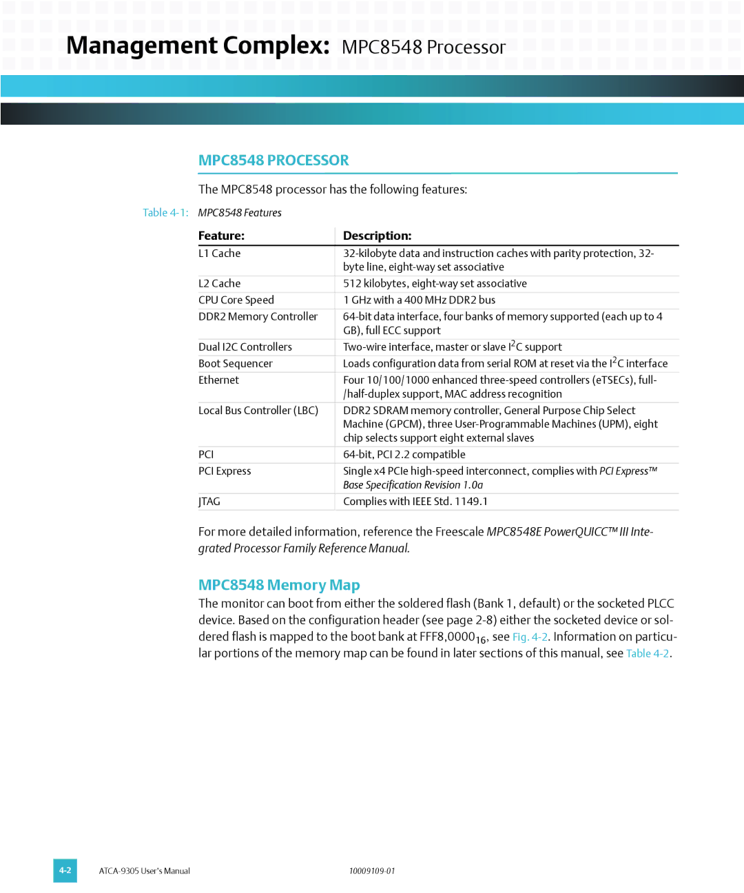
Management Complex MPC8548 Processor
MPC8548 Processor
Jtag
Hex Physical Access See Address Mode Register Description
MPC8548 Ccsrbar 1MB
Hex Physical
See Address Mode Register Description
LED
Chip Selects
Pin Signal
Sdram DDR2 2 GB
Reset Diagram
Ipmp Cpld
Flash
Management Complex Memory
Sdram
KB x 8 optional
GB x
Management Complex PCI
PCI Express
MB x
Management Processor Header and Serial Port
Management Complex I2C Interface
I2C Interface
JTAG/COP Interface optional
Serial Debug Port
MPC8548 PLD Register Summary
Management Processor Cpld
Address Offset hex Mnemonic Register Name See
Hardware Version
Management Processor Cpld MPC8548 PLD Register
Product ID
Bits Function Description
Hardware Configuration
PLL Reset Configuration
PLD Version
Jumper Settings
LED
Reset Event
Reset Command
CAV1CR
WBR
Pqcr
CAV2CR
Reset Command Sticky #1
Reset Command Sticky #2
Boot Device Redirection
Low Frequency Timer 1
Miscellaneous Control
RTM Status
RTM Gpio State
RTM Gpio Control
Frequency Set Register Comments
Cavium 1 Cmul Clock Divisor Control
Cavium 2 Cmul Clock Divisor Control
Jtag
Cavium Gpio Control
Cavium Gpio Data Out
Cavium Gpio Data
LPC Bus Control
IPMP/IPMC Gpio Control
LPC Data
Serial IRQ Interrupt
Blank
Ethernet Switching
Broadcom BCM56802 Switch
Ethernet Interface
Ethernet Transceivers
Ethernet Interface Ethernet Switching
Ethernet Switch Ports
Port Interface Connection
MPC8548 Management Processor Ethernet Address
Vlan Setup
Ethernet Interface MPC8548 Management Processor Ethernet
Ports
Pin P1 Signal P3 Signal
Front Panel Ethernet Ports
TSEC1CHSGND FP1CHSGND
Blank
System Management
Ipmc Overview
System Management Ipmi Messaging
Ipmi Messaging
Hex Code Values Name Type
OEM
Ipmi Completion Codes
Code Description
Ipmb Protocol
System Management Ipmb Protocol
Byte Bits
System Management Sipl Protocol
Sipl Protocol
System Management Message Bridging
Message Bridging
B0 xx 01
Command NetFn
System Management Standard Commands
Standard Commands
Cmd
Picmg
OEM Boot Options
System Management OEM Boot Options
Parameter Parameter Data
Watchdog Timer Actions
System Management Ipmc Watchdog Timer Commands
Ipmc Watchdog Timer Commands
Watchdog Timer Use Field and Expiration Flags
Monitor Support for Watchdog Timer
Watchdog Timer Event Logging
Using the Timer Use Field and Expiration Flags
Monitor Post Time-out
Set Watchdog Timer Command
Reset Watchdog Timer Command
Type Byte Data Field
9Set Watchdog Timer Command
Get Watchdog Timer Command
System Management Ipmc Watchdog Timer Commands
Reference LEDs Hex Designator Description
System Management FRU LEDs
FRU Leds
OOS
Get LED Color Capabilities Command
Get FRU LED Properties Command
LED ID
Response Data
Set FRU LED State Command
Get FRU LED State Command
Function is FBh
System Management FRU LEDs
System Management Vendor Commands
Vendor Commands
Get Status
Carrier controller
Get Serial Interface Properties
Set Serial Interface Properties
Get Debug Level
Set Debug Level
Get Hardware Address
Set Hardware Address
Get Handle Switch
Set Handle Switch
Get Payload Communication Time-Out
Enable Payload Control
Set Payload Communication Time-Out
Reset Ipmc
Disable Payload Control
Hang Ipmc
Bused Resource
Bused Resource Status
Graceful Reset
Diagnostic Interrupt Results
Get Payload Shutdown Time-Out
Set Payload Shutdown Time-Out
Set Local FRU LED State
Get Local FRU LED State
Update Discrete Sensor
Update Threshold Sensor
System Management Boot Device Redirection BDR
Boot Device Redirection BDR
4Boot Device Diagram
System Management Message Listeners
Payload Reset Indication
Payload Reset Indication Clear
Message Listeners
Add Message Listener
Remove Message Listener
Get Message Listener List
System Management System Firmware Progress Sensor
System Firmware Progress Sensor
System Management Entities and Entity Associations
Entities and Entity Associations
Sdram Post
Sdram Post
Sensors and Sensor Data Records
Sensor Event Reading Enity Entity Name Type Instance Gen
Post
Byte Field Description
System Management FRU Inventory
FRU Inventory
System Management E-Keying
Keying
Base Point-to-Point Connectivity
System Management HPM.1 Firmware Upgrade
HPM.1 Firmware Upgrade
Field Value Description
System Management Ipmc Headers
HPM.1 Reliable Field Upgrade Procedure
Pin Signal Direction
Ipmc Headers
Blank
Pin Signal Insertion Sequence
Back Panel Connectors
Zone
Enable a
Back Panel Connectors Zone
Enableb
P10CHSGND
Row Interface
Ipmbrtmsdabuff 33VMPRTM
Rtmrst
12VRTM
COMMAND-LINE Features
Management Processor Monitor
Boardpreinit
Management Processor Monitor Command-Line Features
LED Code Power-up Status LED Value
Serialinit
Management Processor Monitor Basic Operation
Basic Operation
Post Diagnostic Results
2Power-up/Reset Sequence Flowchart
Bit Diagnostic Test Description Value
Management Processor Monitor Monitor Recovery
Monitor Recovery and Updates
Monitor Sdram Usage
Updating the Monitor via Tftp
Recovering the Monitor
Resetting Environment Variables
Address Range hex Device
Monitor Command Reference
Management Processor Monitor Monitor Command
Command Syntax
Management Processor Monitor Boot Commands
Boot Commands
Bootvx
Bootv
Dhcp
Rarpboot
Tftpboot
Memory Commands
Management Processor Monitor File Load Commands
File Load Commands
Loadb
Cmp
Management Processor Monitor Memory Commands
Find
Definition
Example
Erase
Management Processor Monitor Flash Commands
Flash Commands
Flinfo
Protect
Management Processor Monitor EEPROM/I2C Commands
EEPROM/I2C Commands
Eeprom
Imd
Icrc32
Iloop
Imm
Bootdev
Management Processor Monitor Ipmc Commands
Ipmc Commands
Iprobe
Ipmchpmfw
Fruinit
Fruled
Sensor
Printenv
Environment Parameter Commands
Management Processor Monitor Environment Parameter
Saveenv
Test Commands
Management Processor Monitor Test Commands
Other Commands
Management Processor Monitor Other Commands
Isdram
Help
Iminfo
Loop
Pci
Phy
Run
Reset
Ping
Script
Version
Switchreg
Sleep
Vlan
Management Processor Monitor MPC8548 Environment
MPC8548 Environment Variables
Atca
Download Formats
Management Processor Monitor Troubleshooting
9600 bps, no parity, 8 data bits, 1 stop bit
Binary
Management Processor Monitor Download Formats
Motorola S-Record
Blank
Acronyms
GbE
PCIe
SPI-4.2
Index
Air flow rate
Index
Watchdog timer
Blank
10009109-01
E R S O N. C O N S I D E R I T S O L V E D